TM 990 Series 16-bit Microcomputer Modules
![]() Description
Description
![]() Modules and Associated Documentation I Have
Modules and Associated Documentation I Have
![]() Firmware and Software I Have
Firmware and Software I Have
![]() Other Documentation I Have
Other Documentation I Have
![]() Other Documentation Available on the Internet
Other Documentation Available on the Internet
![]() Using VDP Interrupts - Tutorial
Using VDP Interrupts - Tutorial
![]() Connecting a Serial Mouse
Connecting a Serial Mouse
![]() TM 990 Etch-a-Sketch
TM 990 Etch-a-Sketch
![]() Eyeballing for Donations
Eyeballing for Donations
![]() TM 990/510 4-Slot Backplane PCBs Available
TM 990/510 4-Slot Backplane PCBs Available
![]() Other Interesting Bits
Other Interesting Bits
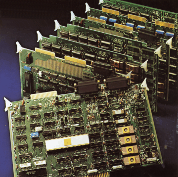 |
The TM 990 Series 16-bit Microcomputer Modules were marketed by Texas Instruments in the early 1980's. The TM 990 range offers a do-it-yourself building block approach to solving application problems. Based around the 16-bit TMS 9900 microprocessor family, the TM 990 modules offer traditional minicomputer power (for the time!) for dedicated controller applications. The modules were often used in factory automation schemes as remote, intelligent, cost-effective stations, for prototyping, and for test equipment to improve production. The TM 990 range includes a low-cost development system which uses audio cassettes for storage and allows programming of EPROMs. The TM 990/302 Software Development Board, populated with appropriate firmware, supports 9900 Assembler and Power BASIC programming. Power BASIC has a number of extensions which enable full manipulation of the hardware resources of a 9900-based system. Interrupts can be handled within its high-level environment or transparently in assembler language. Microprocessor Pascal, both interpretive and compilative versions, was also available. If you have any TM 990 equipment or documentation I'd be interested in hearing from you, possibly with a view to sharing information and swapping EPROM images and software. Contact me at ti99@stuartconner.me.uk. Latest! Remanufactured TM 990/510 4-slot backplane PCBs now available. Contact me for details. |
| Module | Hardware/Firmware | Documentation |
TM 990/100MA Microcomputer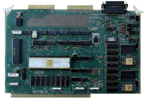 • TMS 9900 16-bit CPU • Up to 1K byte of RAM • Up to 8K bytes of EPROM • DMA to off-board and on-board memory (requires external control circuitry • TMS 9901 programmable system interface • One serial I/O port using TMS 9902 asynchronous communications controller (or TMS 9903 synchronous communications controller optional plug-in replacement) • Two programmable interval timers • Prototyping area for custom applications |
TM 990/100MA Microcomputer, with: • 8 off TMS 4042* (256 × 4) RAMs • 2 off 2708 (1K × 8) EPROMs with TIBUG Monitor (TM 990/401-1 Rev. A, locations U42 and U44) * Two RAM ICs dead when I obtained the board, so have fitted compatible AM9111 (P2111) devices. The memory decode PROM fitted at location U17 is labelled "991575". The I/O decode PROM fitted at location U23 is labelled "991574". RS-232 connection to PC: 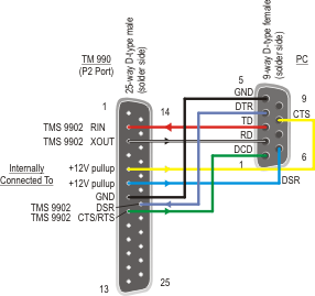
|
TM 990/401-1 TIBUG Monitor Listing (June 1977, MP324) [for the TM 990/100 microcomputer, /401-3 version for the TM 990/101 is slightly different] T-Bus specification from Microsystems Designers Handbook |
TM 990/101MA Microcomputer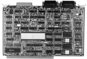 • TMS 9900 16-bit CPU • Up to 4K bytes of RAM • Up to 8K bytes of EPROM • DMA to off-board and on-board memory (requires external control circuitry • TMS 9901 programmable system interface • Two serial I/O ports using TMS 9902 asynchronous communications controllers (one TMS 9903 synchronous communications controller optional plug-in replacement) • Three programmable interval timers • Edge-triggered interrupt, with software reset • CPU-addressable LED and DIP switch for customer applications |
TM 990/101MA Microcomputer, with: • 8 off 2114* (1K × 4) RAMs • 2 off 2708 (1K × 8) EPROMs with TIBUG Monitor (TM 990/401-3 Rev. A, locations U42 and U44 [hex dumps]) • 2 off 2708 (1K × 8) EPROMs with Line-By-Line Assembler (TM 990/402-1, locations U43 and U45 [hex dumps]) * No RAMs fitted when I obtained the board, so have fitted compatible U214D20 devices from www.andysarcade.net. The memory decode PROM fitted at location U19 is labelled "991588". RS-232 connection to PC: same as for the TM 990/100 board above |
TM 990/101MA Microcomputer User's Guide (March 1980, MP337) (or selected scanned pages
from later May 1980 version) TM 990/101MA page from Microsystems Designers Handbook TM 990/402 Line-By-Line Assembler User's Guide (November 1977, MP325) (includes software listing) T-Bus specification from Microsystems Designers Handbook |
TM 990/101MB Microcomputer As TM 990/101MA above, but with • Up to 16K bytes of RAM • Up to 32K bytes of EPROM |
This module was bought as a spare part for a Varian 120/160/180 XP ion implanter, where it is used as part of the control system. The board is fitted with: • 2 off Intel D2732A (4K × 8) EPROMs, containing a copy of the TIBUG Monitor plus Varian software • 1 off Motorola M5M5165P-10L (8K × 8) RAM • 1 off STM MK48T02B-15 (2K × 8) TimeKeeper RAM A couple of tracks on the board have been cut and jumper wires soldered on. These are to (1) configure the two RAM ICs into a 2K × 16 memory area plus 6K × 8 memory area configuration, and (2) to invert address line A10 applied to the TimeKeeper RAM to move the bytes that contain the clock information from the top of the RAM memory area to the middle (with the memory configuration used by Varian, the top of the RAM memory area is at the top of the memory map, which contains the Load interrupt vector). Capacitors are fitted at positions C18 and C23 to debounce the /PRES.B and /RESTART.B inputs and to force a power-on reset. The memory decode PROM fitted at location U19 contains the memory map data specified in the addendum to the User Guide - so the PROM is likely to be original. |
TM 990/101MB Addendum to the TM 990/101MA User Guide |
TM 990/201-43 Memory Expansion Module • 32K bytes of TMS 2716 EPROM • 16K bytes of TMS 2114 static RAM • Fully socketed • Jumper selectable access time • TTL-compatible interface |
TM 990/201-43 Memory Expansion Module, with: • 16 off 2716 (2K × 8) EPROMs (originally with TMS 5100 and TMS 5200 voice synthesis processor data programming firmware, locations U56 to U70, labelled "C-V3 1983 TI", plus location U71, labelled "RM CS" [hex dumps]) • 32 off 2114* (1K × 4) RAMs * Original RAMs fitted are actually compatible TMM314APL-1 devices. |
TM 990/201 & 206 Expansion Memory Modules User's Guide TM 990/201 page from Microsystems Designers Handbook (page includes DIP switch settings for RAM and EPROM memory map) |
TM 990/302 Software Development Module • Stand-alone software development system supporting program generation, editing, assembly, debugging and EPROM programming • For use with either TM 990/100M or TM 990/101M microcomputer modules • Provides dual or single audio cassette interface, both static RAM and ROM memory and hardware circuitry for programming EPROMs • Programming options - TMS 2708, TMS 2716, TMS 2508, TMS 2516, TMS 2532 • 4K × 16 EPROM or preprogrammed ROM • 2K × 16 RAM • Memory expandability for additional performance - TM 990/201, TM 990/206 or TM 990/203 • Optional Power BASIC development software residing in ROM (12K bytes) |
TM 990/302 Software Development Module, with: • 4 off 2716 (2K × 8) EPROMs with Software Development Module firmware (locations U14 to U17, labelled "2212004-01 to 04, R1.5" [hex dumps]*) • 8 off 2114** (1K × 4) RAMs • TM 990/514 EPROM Programming Personality Module (for 2708 and 2716 EPROMs) • TM 990/515 EPROM Programming Personality Module (for 2508, 2516 and 2532 EPROMs) * The module was it seems used in a system with the Development Power BASIC software as a handwritten paper with the board notes how to swap these EPROMs for the TM 990/451 Development Power BASIC and TM 990/452 Development Support Option EPROMs, and the EPROMs are fitted in ZIF sockets plugged into the board so they were presumably removed and replaced frequently. ** One RAM was faulty and I have replaced it with a compatible U214D20 device. The memory decode PROM fitted at location U28 is labelled "1212016" [hex dump]. Location XU12 still contains the "2212017 U12" PROM needed to use the module with the TM 990/100 microcomputer (see the Hardware User's Guide, section 2.5.2). The board requires a 35 - 55V dc power supply from which to derive the +25V programming pulses for the EPROMs. I have used an Ault Model PW118 48V supply found on eBay. |
TM 990/302 Software Development Module User's Guide (June 1980, MP343) TM 990/302 Hardware User's Guide (July 1980, MP344 Rev. C) (includes circuit diagrams) TM 990/514 and TM 990/515 EPROM Personality Programming Cards (November 1978, MPB12) TM 990/302 page from Microsystems Designers Handbook |
TM 990/305 I/O Expansion Module • Combination memory and I/O module • Memory capacity up to 16K bytes using TMS 2516 EPROMs, up to 32K bytes using TMS 2532 EPROMs, or up to 16K bytes using TMS 4016 RAMs • Memory map configuration is jumper selectable • 32 optically isolated I/O lines: 16 are dedicated input lines and 16 are user-configurable I/O lines • Designed to accommodate pin-compatible static RAMs |
TM 990/305 I/O Expansion Module, with: • 8 off 4016* (2K × 8) RAMs • 16 off TIL 117 opto-isolators • 4 off TIL 119 opto-isolators * The TMS 4016-45NL devices originally fitted were working fine but the pins were quite badly tarnished. It seems that the pins had also become quite brittle as a couple of pins broke off all but two of the devices when cleaning them. Replacement TMS 4016-25NL devices are now fitted from www.syracusesemiconductors.com. |
TM 990/305 Combination Memory and I/O Expansion Module (April 1979, MPB28) TM 990/305 page from Microsystems Designers Handbook |
TM 990/1241S (RTI-1241S) Combination Analogue I/O Interface Module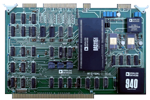 • Up to 32 single-ended or 16 differential inputs to 12-bit A/D converter, with software-programmable gain • Two 12-bit D/A outputs • On-board 10V precision reference • Memory-mapped I/O interface • Made by Analog Devices |
TM 990/1241S (RTI-1241S) Combination Analogue I/O Interface Module, with • Optional ±15V DC-DC converter • Optional 4-20mA current loop V to I converter |
Analog Devices RTI-1241S Module Datasheet Analog Devices DAS1151 A/D Converter Datasheet Analog Devices AD562 D/A Converter Datasheet Analog Devices 940 DC-DC Converter Datasheet |
| TM 990/511 Extender Board • Extender board for operating TM 990 modules outside the card cage |
TM 990/511 Extender Board | TM 990/511 Extender Board (October 1977, MP333) |
TM 990/512 Universal Prototyping Board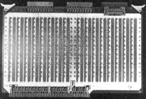 • Universal prototyping board allows custom interface to TM 990 bus • Has GND and 5V planes, two power strips for ±12V, plus two power strips for user-selectable voltage option |
TM 990/512 Universal Prototyping Board | - |
TM 990/520 8-Slot Card Cage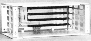 (photo shows 4-slot TM 990/510 card cage) • 8-slot card cage with 0.75 inch board separation • Back panel contains address bus, data bus, interrupt and control lines to permit memory, I/O and DMA expansion of CPU modules • 10-terminal barrier strip on back panel permits connection of the following signals as required: Reset, Restart, ±5V, ±12V, ±15V, GND |
TM 990/520 8-Slot Card Cage Remanufactured TM 990/510 4-slot backplane PCBs are now available. Contact me for details. |
TM 990/510, 520 Card Cages (February 1979, MP341) |
TM 990 IDE Interface Module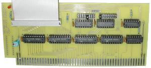 • 16-bit IDE interface module • Tested with several hard disks and CF adapters/cards • Memory mapped I/O, memory map configuration is jumper selectable on a 1K byte boundary |
IDE interface module. Designed by me, with PCB manufactured through ExpressPCB. Have developed software to save/load memory to files on a disk, format a disk, catalogue a disk, display drive information, explore a disk sector-by-sector, and so on. Further work will be to enable the system to boot into a disk-based operating system. |
Hardware documentation Source code |
TM 990 64K Memory Module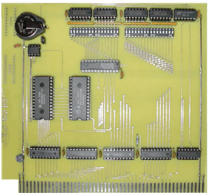 • 64K byte battery-backed RAM module • Memory address space split into 16 4K blocks, each of which can be enabled/disabled and write-protected using DIP switches |
64K byte battery-backed RAM module. Designed by me, with PCB manufactured through ExpressPCB. Tacking a 16 segment bar graph LED onto the output of the address decoder gives a useful visual indication of which memory block(s) most memory accesses are taking place in. |
Hardware documentation |
TM 990 Video Display Processor and Sound Module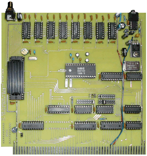 • TMS 9918A video display processor • 16K byte video RAM • NTSC composite video output • Commodore 6581 SID (Sound Interface Device) • Built-in audio amplifier and speaker • Memory mapped I/O, memory map configuration is jumper selectable on a 1K byte boundary |
Video display processor and sound module, using a TMS 9918A VDP and Commodore 6581 SID sound chip. Designed by me, with PCB manufactured through ExpressPCB.  [Yin-Yang based on code by Matthew Hagerty] Simple demo of video and sound capability available here. |
Hardware documentation TMS 9918A/TMS 9928A/TMS 9929A Video Display Processors Manual (November 1982, MP010A) SID 6581 Data Sheet There is a tutorial on using the VDP interrupts below. |
At https://archive.org/search.php?query=tms9900:
In the 99'er magazine (November 1982):
Other brochures/articles/pamphlets:
The TMS 9918A video display processor (VDP) on my TM 990 Video Display Processor and Sound module generates an interrupt at the end of each video frame (every 1/60th of a second). This is a short tutorial on how to use this interrupt to perform a periodic task such as move sprites or process a sound list. For the purposes of this tutorial, a simple example is used: print a message to the RS-232 terminal every 5 seconds.
The following points provide an overview of how the VDP interrupt is set up and processed. A general understanding of how the TMS 9900 processes interrupts is assumed (see the TMS 9900 Microprocessor Data Manual, Section 2.2 if required).
TIBUG has to be modified to set the interrupt 2 workspace pointer (WP) and program counter (PC) vectors to link to an ISR. As these vectors are in read-only memory, they cannot be modified to link to wherever in memory an ISR provided by an application might end up being stored. Instead, an approach is taken where the vectors link to a simple ISR added to the end of the TIBUG code (so the position of this is fixed in memory), then an application 'hooks' its own ISR into the TIBUG ISR. This is a similar approach used by the TI-99/4A home computer.
So, TIBUG needs to define a location for the application ISR hook and the TIBUG ISR workspace. These can be at the top of memory, just below the RAM area already used by TIBUG.
APISRHK EQU >FF7C (2 bytes) (Application ISR hook)
ISRREGS EQU >FF7E (32 bytes, 16 registers) (Workspace for TIBUG ISR)
Then the WP/PC vectors for interrupt 2 have to be defined. When an interrupt level 2 occurs and is enabled by the processor interrupt mask, the processor performs a context switch (in effect, a BLWP instruction) to these vectors and forces the interrupt mask to a value one less than the level of the interrupt being serviced.
AORG >0000
DATA MREGS,INIT WP/PC level 0 interrupt (reset).
DATA ... WP/PC level 1 interrupt - external.
DATA ISRREGS,ISREP WP/PC level 2 interrupt - external - TMS 9918 on VDP and Sound module.
...
The TIBUG ISR checks if an application has stored the address of its ISR at location APISRHK, and if it has (that is, if the word at location APISRHK is non-zero), it branches to the application ISR. The word at location APISRHK therefore has to be cleared during TIBUG's initialisation routine such that the default is for an application ISR not to be present.
INIT CLR @APISRHK Clear application ISR hook.
LI R12,ASR
...
Finally comes TIBUG's ISR. This first reads the VDP status register to clear the VDP interrupt (this is done in the TIBUG ISR such that the interrupt is cleared irrespective of whether or not an application ISR is executed). The ISR then checks the value at the application ISR hook address. If it is non-zero then the code branches to the application ISR. If it is zero then the code returns from the ISR, which also restores the interrupt level in use by the code running at the time the interrupt occurred.
VDPS EQU >E406 Address to read VDP status register.
ISREP MOVB @VDPS,R10 Read VDP status register to clear VDP interrupt.
MOV @APISRHK,R10 Get application ISR hook. Zero?
JNE ISREP01 No, jump.
RTWP Yes, return from ISR. Also restores interrupt level.
ISREP01 B *R10 Jump to address of application ISR hook.
The application code needs to cover two areas: (1) It needs an ISR that is called by the TIBUG ISR. In this tutorial, the ISR is to print a message to the terminal every 5 seconds. (2) It needs code to hook in the application ISR and to configure the VDP, the TMS 9901 and the processor to generate, prioritise and respond to the interrupts. Without the latter, even though the ISRs are in place, no interrupts will actually reach the processor.
Looking at the application ISR first, it is called from the TIBUG ISR (once the hook address is set up), and uses the same workspace ISRREGS as the TIBUG ISR. We need to continue using this workspace as it contains the PC, WP and ST of the code that was interrupted and that we need to return to. The ISR uses a simple counter (initialised in the application code) to count the interrupts. A count of 300 with 60 interrupts per second gives a timer of 5 seconds. Until the timer expires, the ISR simply uses an RTWP to exit the ISR and return to the code that was previously running.
TMRCNT EQU 300 Timer count to use. 300 = 5 seconds.
APPISR DEC R0 Decrement count. Timer expired?
JEQ APP1 Yes, print message then reinitialise.
RTWP No, return.
When the timer expires, the ISR jumps to APP1 to print the message to the terminal. To print the message it uses TIBUG XOP 14 (write message to terminal), but this XOP uses workspaces that TIBUG uses while it is running and we don't know what TIBUG will be doing when an interrupt occurs (an interrupt might occur while TIBUG is actually already in the XOP 14 routine while responding to user input). Specifically, XOP 14 uses the TIBUG XREGS workspace, and XOP 14 calls XOP 12 which uses the IREGS workspace. While TIBUG is waiting for user input, it is calling XOP 11 (which uses workspace EREGS) which in turn calls XOP 13 (which uses IREGS) followed by an XOP 12 (which also uses IREGS). The impact of this is that before calling XOP 14, the ISR first needs to save the PC, WP and ST stored in registers R13, R14 and R15 of the IREGS and XREGS workspaces, plus the other registers that are used by the XOPs, as these will be overwritten when the ISR calls XOP 14. After the XOP 14 call, the ISR then restores these workspace registers. Finally, the ISR re-initialises the timer count before returning with an RTWP.
APP1 LI R1,TMPREGS Address of temporary buffer.
LI R2,>FFC6+20 Address of R10 in TIBUG IREGS workspace.
MOV *R2+,*R1+ Save R10 of IREGS.
MOV *R2+,*R1+ Save R11 of IREGS.
MOV *R2+,*R1+ Save R12 of IREGS.
MOV *R2+,*R1+ Save R13 of IREGS.
MOV *R2+,*R1+ Save R14 of IREGS.
MOV *R2+,*R1+ Save R15 of IREGS.
LI R2,>FFD4+18 Address of R9 in TIBUG XREGS workspace.
MOV *R2+,*R1+ Save R9 of XREGS.
MOV *R2+,*R1+ Save R10 of XREGS.
MOV *R2+,*R1+ Save R11 of XREGS.
MOV *R2+,*R1+ Save R12 of XREGS.
MOV *R2+,*R1+ Save R13 of XREGS.
MOV *R2+,*R1+ Save R14 of XREGS.
MOV *R2,*R1 Save R15 of XREGS.
XOP @MSGTXT,14 Print message to terminal.
LI R1,TMPREGS Address of temporary buffer.
LI R2,>FFC6+20 Address of R10 in TIBUG IREGS workspace.
MOV *R1+,*R2+ Restore R10 of IREGS.
MOV *R1+,*R2+ Restore R11 of IREGS.
MOV *R1+,*R2+ Restore R12 of IREGS.
MOV *R1+,*R2+ Restore R13 of IREGS.
MOV *R1+,*R2+ Restore R14 of IREGS.
MOV *R1+,*R2+ Restore R15 of IREGS.
LI R2,>FFD4+18 Address of R9 in TIBUG XREGS workspace.
MOV *R1+,*R2+ Restore R9 of XREGS.
MOV *R1+,*R2+ Restore R10 of XREGS.
MOV *R1+,*R2+ Restore R11 of XREGS.
MOV *R1+,*R2+ Restore R12 of XREGS.
MOV *R1+,*R2+ Restore R13 of XREGS.
MOV *R1+,*R2+ Restore R14 of XREGS.
MOV *R1,*R2 Restore R15 of XREGS.
LI R0,TMRCNT Re-initialise timer count and return.
RTWP
MSGTXT BYTE >D,>A
TEXT '5 SECONDS ELAPSED'
BYTE >D,>A
BYTE 0
EVEN
TMPREGS BSS 26 Temporary storage of TIBUG registers.
The second section of code to hook in the application ISR and configure the VDP, the TMS 9901 and the processor is standard standalone code that starts by defining its workspace.
LWPI WSREGS Set workspace.
...
(at end of code)
WSREGS BSS 32 Application workspace.
We then need to disable all interrupts while we set things up.
LIMI 0 Disable all other interrupts while setting up.
Next, we initialise the timer count in the application ISR ready for when the first interrupt occurs.
LI R0,TMRCNT Seed timer in application ISR (R0 of workspace ISRREGS).
MOV R0,@ISRREGS
The address of the application ISR is stored in the application ISR hook in the TIBUG RAM area. This is the address that the TIBUG ISR will branch to.
LI R0,APPISR Load address of application ISR.
MOV R0,@APISRHK Store address in application ISR hook.
When the TMS 9901 is reset, it is put into clock mode and all interrupts are masked. The TMS 9901 needs to be switched to interrupt mode and interrupt INT2 unmasked.
LI R12,>0100 Address TMS 9901 on CRU interface.
SBZ 0 Set TMS 9901 to interrupt mode.
SBO 2 Unmask INT2.
The Interrupt Enable bit in VDP register 1 is next set.
VDPA EQU >E402 Address to write to VDP register or to write VRAM address.
LI R0,>01E0 Set VDP to use 16K RAM and enable VDP interrupts.
ORI R0,>8000 Set MS bit to write to register.
SWPB R0 Move VDP register value into MSB of word.
MOVB R0,@VDPA Write VDP register value to VDP.
SWPB R0 Move VDP register number into MSB of word.
MOVB R0,@VDPA Write VDP register number to VDP.
Set the processor interrupt mask.
LIMI 2 Set processor to respond to interrupts 0 - 2.
From this point, VDP interrupts are being generated and handled by the processor which calls the INT2 ISR in TIBUG, which then branches to the application ISR. If the application ISR hook had not been set up, the TIBUG ISR would just clear the VDP interrupt and exit the ISR.
Finally, the application returns to TIBUG. No matter what the user then does in TIBUG, a message should be displayed on the terminal every 5 seconds.
B @>0080 Return to TIBUG.
| A standard, old PC serial mouse can be connected to the second RS-232 port (port P3) on the TM 990/101M module using the adapter shown on the right to swap a few of the RS-232 port pins around. | 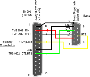 |
| The listing below is for a simple sketch program which uses the mouse to draw a picture on the VDP screen using a sprite as the mouse pointer. The listing also provides an example of how to initialise and control the RS-232 port, and how to plot individual pixels with the TMS 9918A VDP in graphics 2 mode. I've tried two serial mice which both work - labelled on the bottom as a Microsoft "Serial Mouse 2.1A", and a Microsoft "Serial - PS/2 Compatible Mouse". |  |
*********************************************************************************************************
*Experiment using a PC serial mouse to implement a simple sketch program on the TMS9918A VDP (which is
*configured in graphics 2 mode, giving a resolution of 256 x 192).
*Use the mouse to move a sprite mouse pointer around the screen.
*Click the left mouse button to colour pixels as you go.
*Click the right mouse button to cycle through the 14 pixel colours (excluding transparent and black).
*Click the left and right mouse buttons together to clear the screen and start again.
*
*Mouse details reference: www.kryslix.com/nsfaq/Q.12.html
*TMS9918A VDP datasheet: http://ftp.whtech.com/datasheets%20and%20manuals/Datasheets%20-%20TI/TMS9918.pdf
*********************************************************************************************************
AORG >2000
*************
*Definitions.
*************
*Graphics 2 mode storage in VRAM.
PNTBA EQU >1800 Pattern name table base address.
PGTBA EQU >0000 Pattern generator table base address.
CTBA EQU >2000 Colour table base address.
SATBA EQU >1B00 Sprite attribute table base address.
SGTBA EQU >3800 Sprite generator table base address.
*Memory mapped I/O definitions.
VDPREG EQU >E402 VDP VRAM address and register access address.
VRAMW EQU >E400 VDP VRAM data write address.
VRAMR EQU >E404 VDP VRAM data read address.
LWPI MYWS Load workspace.
************************
*Set up Graphics 2 mode.
************************
*Load VDP registers.
START BL @LOADER
BYTE >02,>80 Register 0 - graphics 2 mode, external video off.
BYTE >80,>81 Register 1 - 16K, no display, no interrupt, graphics 2, size & mag = 0.
BYTE >06,>82 Register 2 - PNTBA = >1800. Pattern name table.
BYTE >FF,>83 Register 3 - CTBA = >2000. Colour table.
BYTE >03,>84 Register 4 - PGTBA = >0000. Pattern generator table.
BYTE >36,>85 Register 5 - SATBA = >1B00. Sprite attribute table.
BYTE >07,>86 Register 6 - SGTBA = >3800. Sprite generator table.
BYTE >00,>87 Register 7 - Backdrop=background colour.
DATA 0
*Clear the sprite generator table (SGT) and sprite attribute table (SAT).
LI R7,VRAMW
LI R8,SGTBA+>4000 Reference SGT. Add >4000 for VDP write operations.
BL @SENDAD Send VDP address.
LI R8,256*8 Do 256 8-bit patterns.
KILSGT MOVB @B00,*R7 Null out the pattern.
DEC R8 Count it.
JNE KILSGT Loop till all done.
LI R8,SATBA+>4000 Reference SAT. Add >4000 for VDP write operations.
BL @SENDAD Send VDP address.
LI R8,32*8 Kill off all 32 sprite planes.
LI R6,>D000 Fill it full of sprite terminators.
KILSAT MOVB R6,*R7 Clear SAT.
DEC R8 Count it.
JNE KILSAT Loop till all done.
*Set up pattern name table.
LI R8,PNTBA+>4000 Reference PNT. Add >4000 for VDP write operations.
BL @SENDAD Send VDP address.
SETO R11 Reset count.
INIPNT INC R11 Next pattern.
SWPB R11 Position LS byte.
MOVB R11,*R7 Write it.
SWPB R11 Restore R11.
CI R11,3*256 Done all entries?
JL INIPNT No, loop around.
*Set up pattern generator table.
LI R8,PGTBA+>4000 Reference PGT. Add >4000 for VDP write operations.
BL @SENDAD Send VDP address.
LI R11,3*256*8 Set count.
KILPGT MOVB @B00,*R7 Reset entry.
DEC R11 Done all entries?
JNE KILPGT No, loop around.
*Set up colour table.
LI R8,CTBA+>4000 Reference CT. Add >4000 for VDP write operations.
BL @SENDAD Send VDP address.
CLR R1 Clear R1 because we'll be shifting left.
MOVB @MPTSAT+3,R1 Get initial mouse pointer sprite colour.
SLA R1,4 Shift to left nibble to align with foreground colour in CT.
MOVB R1,@MSCOL Store initial mouse pointer colour.
LI R11,3*256*8 Set count.
INICT MOVB R1,*R7 Set colour to initial mouse pointer sprite colour.
DEC R11 Done all entries?
JNE INICT No, loop around.
*Re-enable display.
BL @LOADER
BYTE >C0,>81
DATA 0
***********************************************************
*Define mouse pointer sprite and place at middle of screen.
***********************************************************
*Write character pattern to the sprite generator table.
LI R8,SGTBA+>4000 Reference SGT. Add >4000 for VDP write operations.
BL @SENDAD Send VDP address.
LI R8,8 Do one 8-bit pattern.
LI R6,MPTSPG Pointer to character pattern.
MPTRSG MOVB *R6+,*R7 Write the pattern.
DEC R8 Count it.
JNE MPTRSG Loop till all done.
*Define sprite in the sprite attribute table.
LI R8,SATBA+>4000 Reference SAT. Add >4000 for VDP write operations.
BL @SENDAD Send VDP address.
LI R8,4 4 bytes to write.
LI R6,MPTSAT Pointer to SAT for mouse pointer.
MPTRSA MOVB *R6+,*R7 Write the SAT.
DEC R8 Count it.
JNE MPTRSA Loop till all done.
**********************************************
*Initialise mouse RS-232 port and reset mouse.
**********************************************
*Set auxiliary port P3 to 1200 Baud, 7 data bits, no parity, 1 stop bit.
LI R12,>0180 CRU base address of 9902 for port P3.
SBO 31 Reset 9902. This sets /RTS inactive high, so the RTS output line to -ve voltage.
LI R1,>8200 Control register: 1 stop bit, no parity, 7 data bits (binary 10000010).
LDCR R1,8 Load control register.
SBZ 13 Disable loading of interval register.
LI R1,>01A0 1200 Baud.
LDCR R1,12 Load transmit and receive data rate registers.
BL @DLY1 Mouse needs negative pulse of at least 100ms.
*Toggle RTS output line to +ve voltage to reset mouse.
SBO 16 Set /RTS active low, so the RTS output line to +ve voltage.
*On reset the mouse should send the letter 'M', but it doesn't always seems to send this character
*or indeed any character at all, so just ignore the first character received.
WAIT1 TB 21 Receive buffer register full?
JNE WAIT1 No, loop until a character is received.
SBZ 18 Reset receive buffer register.
*Initialise mouse position to the middle of the screen.
*Mouse position range is twice the screen resolution (twice 192 x 256) to get an adequate movement
*of the mouse. The mouse position will be divided by two to map it to screen coordinates.
*(Can't divide mouse movement by two otherwise very slow movement will result in no movement.)
LI R9,256/2*2 Mouse X position in LSB.
MOV R9,@MSXPOS
LI R9,192/2*2 Mouse Y position in LSB.
MOV R9,@MSYPOS
******************************************
*Wait for a packet of data from the mouse.
******************************************
*Wait for and store a packet of 3 bytes. The first byte of each packet should be a value greater
*than or equal to >40. Check for this to keep reception in sync.
WAIT2 LI R12,>0180 CRU base address of 9902 for port P3.
CLR R1
CLR R2
CLR R3
WAIT3 TB 21 Receive buffer register full?
JNE WAIT3 No, loop until a character is received.
STCR R1,8 Read character into MSB of R1.
SBZ 18 Reset receive buffer register.
CI R1,>4000 Bit set to indicate first byte in packet?
JL WAIT3 No, get another byte.
WAIT4 TB 21 Receive buffer register full?
JNE WAIT4 No, loop until a character is received.
STCR R2,8 Read character into MSB of R2.
SBZ 18 Reset receive buffer register.
WAIT5 TB 21 Receive buffer register full?
JNE WAIT5 No, loop until a character is received.
STCR R3,8 Read character into MSB of R3.
SBZ 18 Reset receive buffer register.
********************************************************
*Determine the mouse movement and update mouse position.
********************************************************
*Determine the X movement.
MOV R1,R5 Copy byte 1.
SLA R5,6 Move MS bits of X movement to top of byte.
A R5,R2 Add to rest of X movement in 2nd byte.
SWPB R2 Move result into LSB.
*Determine the Y movement.
MOV R1,R5 Copy byte 1.
ANDI R5,>0C00 Isolate bits 2 and 3.
SLA R5,4 Shift to move MS bits of Y movement to top of byte.
A R5,R3 Add to rest of Y movement in 3rd byte.
SWPB R3 Move result into LSB.
*Update mouse X position.
MOV @MSXPOS,R9 Get stored mouse X position.
CI R2,128 Is X movement left (-ve) or right (+ve)?
JLE UPDTX1 Jump if to the right.
AI R2,>FF00 Movement is to the left. Change to two's complement word.
A R2,R9 Subtract (add two's complement) movement from mouse X position.
JGT UPDTX2 If position now > 0, it's valid.
JEQ UPDTX2 If position now 0, it's valid.
CLR R9 Result is < 0, so reset position to 0.
JMP UPDTX2
UPDTX1 A R2,R9 Add movement to X position.
CI R9,2*255 If X position > 2*255 then set to 2*255.
JLE UPDTX2
LI R9,2*255
UPDTX2 MOV R9,@MSXPOS Store new mouse X position.
*Update mouse Y position.
MOV @MSYPOS,R9 Get stored mouse Y position.
CI R3,128 Is Y movement up (-ve) or down (+ve)?
JLE UPDTY1 Jump if down.
AI R3,>FF00 Movement is up. Change to two's complement word.
A R3,R9 Subtract (add two's complement) movement from mouse Y position.
JGT UPDTY2 If position now > 0, it's valid.
JEQ UPDTY2 If position now 0, it's valid.
CLR R9 Result is < 0, so reset position to 0.
JMP UPDTY2
UPDTY1 A R3,R9 Add movement to Y position.
CI R9,2*191 If Y position > 2*191 then set to 2*191.
JLE UPDTY2
LI R9,2*191
UPDTY2 MOV R9,@MSYPOS Store new mouse Y position.
***************************
*Move mouse pointer sprite.
***************************
*First byte in SAT is vertical position, second byte is horizontal position.
MOVMS LI R8,SATBA+>4000 Reference SAT. Add >4000 for VDP write operations.
BL @SENDAD Send VDP address.
MOV @MSYPOS,R2 Get stored mouse Y position (which is at twice screen resolution).
DECT R2 Top row of the screen has value -1, so adjust.
SLA R2,7 Move to MSB and divide by 2 to convert to screen resolution.
MOVB R2,*R7 Write the Y mouse position.
MOV @MSXPOS,R2 Get stored mouse X position (which is at twice screen resolution).
SLA R2,7 Move to MSB and divide by 2 to convert to screen resolution.
MOVB R2,*R7 Write the X mouse position.
****************************************************************************
*Check for left and right buttons pressed together. If pressed, clear screen
*and start again.
****************************************************************************
COC @H7000,R1 Check for left and right button indication in 1st byte received.
JNE CLRSCRN Left and right button not both pressed, jump.
B @START Blank display and start again.
CLRSCRN EQU $
***********************************************************************
*Check for right button press. If pressed, change mouse pointer colour.
***********************************************************************
COC @H5000,R1 Check for right button indication in 1st byte received.
JNE UPDCOL1 Right button not pressed, jump.
AB @H10,@MSCOL Right button pressed. Move onto next colour.
JNE UPDCOL Need to wrap colour index back round? No, jump.
MOVB @H20,@MSCOL Reset colour to 2, skipping transparent and black colours.
UPDCOL LI R8,SATBA+>4000+3 Reference colour byte in SAT. Add >4000 for VDP write operations.
BL @SENDAD Send VDP address.
MOVB @MSCOL,R2 Get stored colour.
SRL R2,4 Shift to 2nd nibble to align with colour nibble in SAT.
MOVB R2,*R7 Write new colour to mouse pointer sprite.
UPDCOL1 EQU $
***********************************************************************
*Check for left button press. If pressed, draw pixel at mouse position.
***********************************************************************
COC @H6000,R1 Check for right button indication in 1st byte received.
JNE DRWPX99 Left button not pressed, jump.
*Convert mouse X position to column number and remainder.
MOV @MSXPOS,R2 Get X position (which is at twice screen resolution).
MOV R2,R3 Copy it.
SRL R2,4 Divide by 2 to convert to screen resolution, then divide by 8 to get column number.
SRL R3,1 Divide by 2 to convert to screen resolution.
ANDI R3,>0007 Get 3 LS bits which are the remainder (the pixel 0 to 7 within the 8-pixel column).
*Convert mouse Y position to row number and remainder.
MOV @MSYPOS,R8 Get Y position (which is at twice screen resolution).
MOV R8,R9 Copy it.
SRL R8,4 Divide by 2 to convert to screen resolution, then divide by 8 to get row number.
SRL R9,1 Divide by 2 to convert to screen resolution.
ANDI R9,>0007 Get 3 LS bits which are the remainder (the pixel 0 to 7 within the 8-pixel row).
*Multiply row number by 32, then add column number to get cell number.
SLA R8,5 Multiply row number by 32.
A R2,R8 Add column number.
*Multiply cell number by 8 to get index into entry in the PGT for this cell
*(8 bytes in PGT per cell, 1 per pixel row).
SLA R8,3 Multiply cell number by 8.
*Get current VRAM data from cell number, add new pixel, and write back to VRAM.
A R9,R8 Add Y remainder to get correct byte in PGT for the pixel row.
BL @SENDAD Send cell address to VDP.
CLR R10 Clear pixel mask register. The pixel mask gives the bit to
* set in the PGT byte for the pixel 0 to 7 within the 8-pixel column.
AI R3,MASKTB Add address of pixel mask table base to X remainder.
MOVB *R3,R10 Fetch pixel mask.
MOVB @VRAMR,R3 Get current VRAM data.
SOCB R10,R3 Set pixel bit.
ORI R8,>4000 Set VDP write bit in address.
BL @SENDAD Send address to VDP.
MOVB R3,*R7 Write updated VRAM data.
*Set the colour table entry to the current mouse pointer sprite colour.
AI R8,CTBA-PGTBA Get address of PCT entry.
BL @SENDAD Send address to VDP.
MOVB @MSCOL,*R7 Update colour entry.
DRWPX99 EQU $
********************************
*Loop round and do it all again.
********************************
B @WAIT2
*************
*Subroutines.
*************
*Load the VDP registers from an inline data table.
LOADER MOVB *R11+,@VDPREG Write register data.
C *R11,*R11 Dummy delay for VDP.
MOVB *R11+,@VDPREG Write register number.
MOV *R11,*R11 End of data table?
JNE LOADER No, loop.
INCT R11 Yes, skip data table terminator.
B *R11 Return.
*Send the address in R8 to the VDP.
SENDAD SWPB R8 Position LSB.
MOVB R8,@VDPREG Send LSB.
SWPB R8 Position MSB.
MOVB R8,@VDPREG Send MSB.
B *R11 Return.
*Short delay.
DLY1 SETO R10
DLY11 DEC R10
JNE DLY11
B *R11 Return.
********************
*Workspace and data.
********************
MYWS BSS 32 Workspace.
MSXPOS DATA 0 Mouse X position in LSB.
MSYPOS DATA 0 Mouse Y position in LSB.
MSCOL BYTE 0 Mouse pointer colour.
B00 BYTE 0
B16 BYTE 16
H10 BYTE >10
H20 BYTE >20
H5000 DATA >5000
H6000 DATA >6000
H7000 DATA >7000
*Mouse pointer sprite data.
MPTSPG BYTE >F0,>E0,>E0,>90,>08,>04,>02,>01 Arrow pattern.
MPTSAT BYTE 192/2-1,256/2,>00,>05 Initial position middle of screen, colour light blue.
*Pixel bit mask table.
*Pixel------- 0 1 2 3 4 5 6 7
MASKTB DATA >8040,>2010,>0804,>0201
END
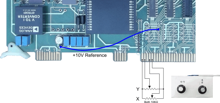
This is a simple project to use the TM 990/1241 Combination Analogue I/O Interface Module. Two rotary potentiometers are connected to the module ADC inputs shown in the diagram below. The position of these is used to control a pen pointer sprite on the VDP screen to form an Etch-a-Sketch. The TMS 9918A VDP is configured in graphics 2 mode.

*********************************************************************************************************
*TM990 Etch-a-Sketch program, using TM990/1241 module to convert analogue inputs from two control
*potentiometers to digital. Picture is plotted using TMS9918A VDP (which is configured in graphics 2 mode,
*giving a resolution of 256 x 192). A sprite is used for the pen pointer.
*Includes commands entered through the RS-232 terminal to raise and lower the pen (so the pointer can be
*moved without drawing), to change the line colour, and to clear the screen.
*********************************************************************************************************
AORG >2000
*************
*Definitions.
*************
*ADC input definitions.
ADCBA EQU >A000 TM990/1241 memory mapped I/O base address.
MUXIPX EQU 9 ADC mux input channel for X potentiometer. (+10V reference is on channel 10.)
MUXIPY EQU 8 ADC mux input channel for Y potentiometer.
MUXST EQU 20 Settling time after changing mux input.
*Graphics 2 mode storage in VRAM.
PNTBA EQU >1800 Pattern name table base address.
PGTBA EQU >0000 Pattern generator table base address.
CTBA EQU >2000 Colour table base address.
SATBA EQU >1B00 Sprite attribute table base address.
SGTBA EQU >3800 Sprite generator table base address.
*VDP memory mapped I/O definitions.
VDPREG EQU >E402 VDP VRAM address and register access address.
VRAMW EQU >E400 VDP VRAM data write address.
VRAMR EQU >E404 VDP VRAM data read address.
*******
*Start.
*******
LWPI MYWS Load workspace.
***********************
*Print welcome message.
***********************
XOP @CLSCRN,14 Clear screen.
XOP @WELCOME,14 Print message.
******************************
*Set default pen status to up.
******************************
START SETO @PENUD Set pen status flag.
XOP @PENUP,14 Print current pen status.
XOP @CRLF,14
************************
*Set up Graphics 2 mode.
************************
*Load VDP registers.
BL @LOADER
BYTE >02,>80 Register 0 - graphics 2 mode, external video off.
BYTE >80,>81 Register 1 - 16K, no display, no interrupt, graphics 2, size & mag = 0.
BYTE >06,>82 Register 2 - PNTBA = >1800. Pattern name table.
BYTE >FF,>83 Register 3 - CTBA = >2000. Colour table.
BYTE >03,>84 Register 4 - PGTBA = >0000. Pattern generator table.
BYTE >36,>85 Register 5 - SATBA = >1B00. Sprite attribute table.
BYTE >07,>86 Register 6 - SGTBA = >3800. Sprite generator table.
BYTE >00,>87 Register 7 - Backdrop=background colour.
DATA 0
*Clear the sprite generator table (SGT) and sprite attribute table (SAT).
LI R7,VRAMW
LI R8,SGTBA+>4000 Reference SGT. Add >4000 for VDP write operations.
BL @SENDAD Send VDP address.
LI R8,256*8 Do 256 8-bit patterns.
KILSGT MOVB @B00,*R7 Null out the pattern.
DEC R8 Count it.
JNE KILSGT Loop till all done.
LI R8,SATBA+>4000 Reference SAT. Add >4000 for VDP write operations.
BL @SENDAD Send VDP address.
LI R8,32*8 Kill off all 32 sprite planes.
LI R6,>D000 Fill it full of sprite terminators.
KILSAT MOVB R6,*R7 Clear SAT.
DEC R8 Count it.
JNE KILSAT Loop till all done.
*Set up pattern name table.
LI R8,PNTBA+>4000 Reference PNT. Add >4000 for VDP write operations.
BL @SENDAD Send VDP address.
SETO R11 Reset count.
INIPNT INC R11 Next pattern.
SWPB R11 Position LS byte.
MOVB R11,*R7 Write it.
SWPB R11 Restore R11.
CI R11,3*256 Done all entries?
JL INIPNT No, loop around.
*Set up pattern generator table.
LI R8,PGTBA+>4000 Reference PGT. Add >4000 for VDP write operations.
BL @SENDAD Send VDP address.
LI R11,3*256*8 Set count.
KILPGT MOVB @B00,*R7 Reset entry.
DEC R11 Done all entries?
JNE KILPGT No, loop around.
*Set up colour table.
LI R8,CTBA+>4000 Reference CT. Add >4000 for VDP write operations.
BL @SENDAD Send VDP address.
CLR R1 Clear R1 because we'll be shifting left.
MOVB @MPTSAT+3,R1 Get initial pen pointer sprite colour.
SLA R1,4 Shift to left nibble to align with foreground colour in CT.
MOVB R1,@CSCOL Store initial pen pointer colour.
LI R11,3*256*8 Set count.
INICT MOVB R1,*R7 Set colour to initial pen pointer sprite colour.
DEC R11 Done all entries?
JNE INICT No, loop around.
*Re-enable display.
BL @LOADER
BYTE >C0,>81
DATA 0
***************************
*Define pen pointer sprite.
***************************
*Write character pattern to the sprite generator table.
LI R8,SGTBA+>4000 Reference SGT. Add >4000 for VDP write operations.
BL @SENDAD Send VDP address.
LI R8,8 Do one 8-bit pattern.
LI R6,MPTSPG Pointer to character pattern.
MPTRSG MOVB *R6+,*R7 Write the pattern.
DEC R8 Count it.
JNE MPTRSG Loop till all done.
*Define sprite in the sprite attribute table.
LI R8,SATBA+>4000 Reference SAT. Add >4000 for VDP write operations.
BL @SENDAD Send VDP address.
LI R8,4 4 bytes to write.
LI R6,MPTSAT Pointer to SAT for pointer.
MPTRSA MOVB *R6+,*R7 Write the SAT.
DEC R8 Count it.
JNE MPTRSA Loop till all done.
*************************************
*Check for command input and process.
*************************************
LI R12,>0080 Set CRU base address to serial port.
MAINLP TB 21 Serial port receive buffer register full?
JNE READPOT No, skip rest of this section.
XOP R2,13 Read character from serial port.
C R2,@UCHAR Character 'U' (pen up)?
JNE NXTCHR1 No jump.
SETO @PENUD Yes, set pen flag.
XOP @PENUP,14 Print current pen status.
XOP @CRLF,14
JMP READPOT
NXTCHR1 C R2,@DCHAR Character 'D' (pen down)?
JNE NXTCHR2 No, jump.
CLR @PENUD Yes, set pen flag.
XOP @PENDN,14 Print current pen status.
XOP @CRLF,14
JMP READPOT
NXTCHR2 C R2,@CCHAR Character 'C' (change colour)?
JNE NXTCHR3 No, jump.
AB @H10,@CSCOL Move onto next colour.
JNE UPDCOL Need to wrap colour index back round? No, jump.
MOVB @H10,@CSCOL Reset colour to 1 (skipping transparent).
UPDCOL LI R8,SATBA+>4000+3 Reference colour byte in SAT. Add >4000 for VDP write operations.
BL @SENDAD Send VDP address.
MOVB @CSCOL,R2 Get stored colour.
SRL R2,4 Shift to 2nd nibble to align with colour nibble in SAT.
MOVB R2,*R7 Write new colour to pen pointer sprite.
XOP @COLOUR,14 Print colour intro text.
SRL R2,7 Shift colour into LS bits, multiplied by 2.
MOV @COLINDX(R2),R3 Get pointer to colour text.
XOP *R3,14 Print colour name text.
XOP @CRLF,14
JMP READPOT
NXTCHR3 C R2,@SCHAR Character 'S' (clear screen and start again)?
JNE READPOT No, jump.
B @START
***********************************
*Read X-Y potentionmeter positions.
***********************************
READPOT BL @READXY
*************************
*Move pen pointer sprite.
*************************
*First byte in SAT is vertical position, second byte is horizontal position.
MOVMS LI R8,SATBA+>4000 Reference SAT. Add >4000 for VDP write operations.
BL @SENDAD Send VDP address.
MOV @CSYPOS,R2 Get the Y position.
DEC R2 Top row of the screen has value -1, so adjust.
SWPB R2
MOVB R2,*R7 Write the Y position.
MOV @CSXPOS,R2 Get the X position.
SWPB R2
MOVB R2,*R7 Write the X position.
***********************************************
*Draw pixel at pointer position if pen is down.
***********************************************
*Check pen status and only draw if pen is down.
MOV @PENUD,R2 Get pen status.
JNE NODRAW Jump if pen is up.
*Convert X position to column number and remainder.
MOV @CSXPOS,R2 Get X position.
MOV R2,R3 Copy it.
SRL R2,3 Divide by 8 to get column number.
ANDI R3,>0007 Get 3 LS bits which are the remainder (the pixel 0 to 7 within the 8-pixel column).
*Convert Y position to row number and remainder.
MOV @CSYPOS,R8 Get Y position.
MOV R8,R9 Copy it.
SRL R8,3 Divide by 8 to get row number.
ANDI R9,>0007 Get 3 LS bits which are the remainder (the pixel 0 to 7 within the 8-pixel row).
*Multiply row number by 32, then add column number to get cell number.
SLA R8,5 Multiply row number by 32.
A R2,R8 Add column number.
*Multiply cell number by 8 to get index into entry in the PGT for this cell
*(8 bytes in PGT per cell, 1 per pixel row).
SLA R8,3 Multiply cell number by 8.
*Get current VRAM data from cell number, add new pixel, and write back to VRAM.
A R9,R8 Add Y remainder to get correct byte in PGT for the pixel row.
BL @SENDAD Send cell address to VDP.
CLR R10 Clear pixel mask register. The pixel mask gives the bit to
* set in the PGT byte for the pixel 0 to 7 within the 8-pixel column.
AI R3,MASKTB Add address of pixel mask table base to X remainder.
MOVB *R3,R10 Fetch pixel mask.
MOVB @VRAMR,R3 Get current VRAM data.
SOCB R10,R3 Set pixel bit.
ORI R8,>4000 Set VDP write bit in address.
BL @SENDAD Send address to VDP.
MOVB R3,*R7 Write updated VRAM data.
*Set the colour table entry to the current pen pointer sprite colour.
AI R8,CTBA-PGTBA Get address of PCT entry.
BL @SENDAD Send address to VDP.
MOVB @CSCOL,*R7 Update colour entry.
NODRAW EQU $
********************************
*Loop round and do it all again.
********************************
B @MAINLP
*************
*Subroutines.
*************
*Load the VDP registers from an inline data table.
LOADER MOVB *R11+,@VDPREG Write register data.
C *R11,*R11 Dummy delay for VDP.
MOVB *R11+,@VDPREG Write register number.
MOV *R11,*R11 End of data table?
JNE LOADER No, loop.
INCT R11 Yes, skip data table terminator.
B *R11 Return.
*Send the address in R8 to the VDP.
SENDAD SWPB R8 Position LSB.
MOVB R8,@VDPREG Send LSB.
SWPB R8 Position MSB.
MOVB R8,@VDPREG Send MSB.
B *R11 Return.
*Read X-Y potentiometer positions from ADC.
READXY LI R1,MUXIPX Select ADC mux X channel.
MOV R1,@ADCBA+>8
LI R1,MUXST Seems to need additional settling time otherwise
LP1 DEC R1 line can be jaggy across full range.
JNE LP1
MOV R1,@ADCBA+>A Send convert command to ADC (write any data).
CLOOPX INV @ADCBA+>C Check status for end of conversion.
JLT CLOOPX Loop until ready.
MOV @ADCBA+>E,R1 Read ADC data.
SRL R1,3 Divide by 8 to reduce 0-2047 range to 0-255.
INV R1 Reverse direction - need max potentiometer reading to be on left of screen.
ANDI R1,>00FF
MOV R1,@CSXPOS Save reading.
LI R1,MUXIPY Select ADC mux Y channel.
MOV R1,@ADCBA+>8
LI R1,MUXST Seems to need additional settling time otherwise
LP2 DEC R1 line can be jaggy across full range.
JNE LP2
MOV R1,@ADCBA+>A Send convert command to ADC (write any data).
CLOOPY INV @ADCBA+>C Check status for end of conversion.
JLT CLOOPY Loop until ready.
MOV @ADCBA+>E,R1 Read ADC data.
SRL R1,3 Divide by 8 to reduce 0-2047 range to 0-255.
CI R1,191 Reading above max Y value of 191?
JLE SAVEY No, jump.
LI R1,191 Set reading to max Y value.
SAVEY MOV R1,@CSYPOS Save reading.
B *R11
********************
*Workspace and data.
********************
MYWS BSS 32 Workspace.
CSXPOS DATA 0 Pen pointer X position in LSB.
CSYPOS DATA 0 Pen pointer Y position in LSB.
CSCOL BYTE 0 Pen pointer colour in MS nibble.
PENUD DATA 0 Pen status - up (>FFFF) or down (>0000).
B00 BYTE 0
H10 BYTE >10
CCHAR DATA 'C'*256
DCHAR DATA 'D'*256
SCHAR DATA 'S'*256
UCHAR DATA 'U'*256
*Pointer sprite data.
MPTSPG BYTE >F0,>E0,>E0,>90,>08,>04,>02,>01 Arrow pattern.
MPTSAT BYTE >00,>00,>00,>05 Initial position top left of screen, colour light blue.
*Pixel bit mask table.
*Pixel------- 0 1 2 3 4 5 6 7
MASKTB DATA >8040,>2010,>0804,>0201
******
*Text.
******
CLSCRN DATA >1B5B,>324A VT100 escape code to erase screen.
BYTE >1B,>5B,>48 VT100 escape code to move cursor to top left.
BYTE 0
WELCOME TEXT 'TM990 ETCH-A-SKETCH, BY STUART CONNER, JULY 2012.'
BYTE >0D,>0A
TEXT 'REQUIRES TM990/1241 ANALOGUE I/O INTERFACE MODULE,'
BYTE >0D,>0A
TEXT 'AND TWO POTENTIOMETERS AS CONTROLS.'
BYTE >0D,>0A
BYTE >0D,>0A
TEXT 'COMMANDS:'
BYTE >0D,>0A
TEXT ' U - PEN UP'
BYTE >0D,>0A
TEXT ' D - PEN DOWN'
BYTE >0D,>0A
TEXT ' C - CHANGE COLOUR'
BYTE >0D,>0A
TEXT ' S - CLEAR SCREEN AND START AGAIN'
BYTE >0D,>0A
CRLF BYTE >0D,>0A
BYTE 0
PENUP TEXT 'PEN IS NOW UP'
BYTE 0
PENDN TEXT 'PEN IS NOW DOWN'
BYTE 0
COLOUR TEXT 'COLOUR IS NOW '
BYTE 0
COL1 TEXT 'BLACK'
BYTE 0
COL2 TEXT 'MEDIUM GREEN'
BYTE 0
COL3 TEXT 'LIGHT GREEN'
BYTE 0
COL4 TEXT 'DARK BLUE'
BYTE 0
COL5 TEXT 'LIGHT BLUE'
BYTE 0
COL6 TEXT 'DARK RED'
BYTE 0
COL7 TEXT 'CYAN'
BYTE 0
COL8 TEXT 'MEDIUM RED'
BYTE 0
COL9 TEXT 'LIGHT RED'
BYTE 0
COL10 TEXT 'DARK YELLOW'
BYTE 0
COL11 TEXT 'LIGHT YELLOW'
BYTE 0
COL12 TEXT 'DARK GREEN'
BYTE 0
COL13 TEXT 'MAGENTA'
BYTE 0
COL14 TEXT 'GREY'
BYTE 0
COL15 TEXT 'WHITE'
COLINDX DATA 0,COL1,COL2,COL3,COL4,COL5,COL6,COL7,COL8
DATA COL9,COL10,COL11,COL12,COL13,COL14,COL15
END
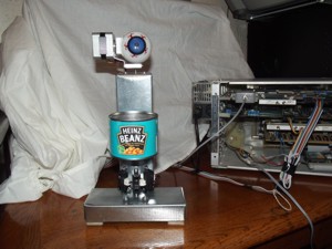
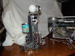
This is a simple little robotics project inspired by the project I saw here.
The device is controlled by a TMS 9900 processor in a modular TM 990 system. Three analogue proximity sensors are connected to a multi-channel A-D converter. The sensors are scanned back and forth and enable a 'target' to be detected and tracked by the eye which swivels horizontally and vertically. When the target gets close enough, the money tin shakes. The project uses four stepper motors, with the stepper motor controller board control inputs connected directly to a TMS 9901.
**************
*Introduction.
**************
*Sweep sensors and record proximity information from each of the three sensors
*for each step of the sweep.
*At the end of each sweep, check the proximity information to determine if a
*target has been detected and in which direction.
*If a target has been detected, store the direction and move the eye
*horizontally to point in that direction during the next sweep. Move the eye
*vertically to 'look up' to the target, looking further up the closer the
*target.
*If the target is very close, move the eye horizontally to look straight
*ahead, move it vertically to look down, and shake the money tin. Then return
*to the previous position. Wait for the target to move back, then come close
*again before shaking the tin again.
*If a target is acquired then lost, return the eye horizontally and vertically
*to look straight ahead.
********************************************************
*Stepper motor controller board connections and details.
********************************************************
*Datasheet: <http://www.hobbytronics.co.uk/robotics/easydriver-stepper-motor>.
*Motor 1 - sensor scan.
*Motor 2 - Eye horizontal motor.
*Motor 3 - Eye vertical motor.
*Motor 4 - Money tin shake motor.
*------------------------------------------------
*Signal Conn. P4 TMS9901 CRU Bit
* Pin Signal
*------------------------------------------------
*Motor 1 DIR - - - 10 - - - - P5 - - - - SBO 21 with R12=>100
*Motor 1 STEP - - - 12 - - - - P6 - - - - SBO 22
*Motor 1 GND - - - 9
*Motor 2 DIR - - - 16 - - - - P3 - - - - SBO 19
*Motor 2 STEP - - - 18 - - - - P4 - - - - SBO 20
*Motor 2 GND - - - 15
*Motor 3 DIR - - - 22 - - - - P1 - - - - SBO 17
*Motor 3 STEP - - - 14 - - - - P2 - - - - SBO 18
*Motor 3 GND - - - 21
*Motor 4 DIR - - - 24 - - - - P7 - - - - SBO 23
*Motor 4 STEP - - - 26 - - - - P8 - - - - SBO 24
*Motor 4 GND - - - 23
*DIR input: low for anticlockwise
* high for clockwise
*Number of motor steps for one full revolution: 200 (1.8° per step)
*Number of motor microsteps per step: 8
****************
*Sensor details.
****************
*Sharp GP2Y0A21YK0F Analogue Distance Sensor, 10 - 80 cm (4 - 32").
*Datasheet: <http://www.hobbytronics.co.uk/datasheets/gp2y0a21yk0f.pdf>.
*According to the datasheet, a measurement is made every 38ms.
*So can take a maximum of 26 samples per second.
*So a sweep of 26 samples should take ~1 second.
*****************
*Sensor geometry.
*****************
*Three sensors are used, spaced 45° apart.
*Scan in an arc of 45°, the sensors will together cover an arc of 135°.
*We'll actually scan in an arc of 26 steps = 46.8° = 140.4° coverage.
*The coverage can be reduced to ignore close objects at the extremities of the
*scan using the SCANIE definition below. So the sensors will still scan 45° so
*that objects between the individual sensor arcs are not missed, but the data
*from the extremeties of the arc will not be checked for a target.
*************
*Definitions.
*************
*ADC input definitions.
ADCBA EQU >A000 TM990/1241 memory mapped I/O base address.
MUXIPSL EQU 8 ADC mux input channel for left sensor.
MUXIPSM EQU 9 ADC mux input channel for middle sensor.
* (+10V reference is wired to channel 10.)
MUXIPSR EQU 11 ADC mux input channel for right sensor.
*Stepper motor definitions.
MSTPDLY EQU >0180 Delay between motor 1 microsteps to give required
* sensor sweep speed.
MINMDLY EQU >0060 Delay between microsteps for eye horizontal and
* vertical motors (2 and 3).
MTINDLY EQU >0070 Delay between motor 4 microsteps to give required
* money tin shake speed.
M1STEPS EQU 26 Steps in arc travelled by sensor motors.
M2STEPS EQU M1STEPS*3 Maximum number of steps in arc travelled by eye
* horizontal motor.
M3STEPS EQU 26 Maximum number of steps in arc travelled by eye
* vertical motor.
M4STEPS EQU 40 Maximum number of steps in arc travelled by money tin
* motor.
*Threshold definitions.
THRSH1V EQU >40 ADC data threshold - if value equal to or above this
* then target assumed detected. (Higher value is closer
* to sensor. Value not linear with distance.)
MINSTPS EQU 5 Minimum number of sensor steps across which a target
* must be found to be valid.
THRSH2V EQU >F0 ADC data second threshold - if value equal to or
* above this then target close enough to trigger
* shaking the money tin.
SCANIE EQU 10 Number of steps at the extremities of the sensor scan
* for which to ignore the data. If this value is 0, the
* data from all 26 sensor scan steps is checked for a
* target. If this value is 5, the data from the
* left-most and right-most 5 sensor scan steps from the
* left and right sensors are not checked for a target.
* (I only put this in because in my little 'computer
* corner' the sensors kept triggering off the curtains,
* so I needed to narrow the sensor range.)
MEYETHV EQU 3 Difference required between eye horizontal and
* vertical required positions and current positions in
* order to move the eye. This stops the eye motors from
* making very small movements after each sensor sweep.
*******
*Start.
*******
AORG >2000
LWPI WSREG Load workspace.
******************************************************************************
*Set up TMS9901 and initialise motor positions. Bring sensor to start of arc.
*The assumed motor start positions is for the middle sensor to be facing
*forwards, the eye to be facing forwards, and the money tin level.
******************************************************************************
LI R12,>100 Base address of TMS9901.
LI R1,M1STEPS/2 Middle sensor is initially facing forwards at
MOV R1,@M1STPOS centre of arc.
LI R1,M2STEPS/2 Eye is initially facing forwards horizontally at
MOV R1,@M2STPOS centre of arc.
MOV R1,@M2TGPOS
LI R1,M3STEPS/2 Eye is initially facing forwards vertically at
MOV R1,@M3STPOS centre of arc.
LI R1,M4STEPS/2 Money tin is initially level.
MOV R1,@M4STPOS
SBZ 22 Set sensor motor STEP low.
SNSMTR1 BL @M1CW Step sensor motor clockwise.
DEC @M1STPOS Decrement sensor motor step position.
JNE SNSMTR1 Repeat until sensor is at start of arc.
******************************************************************************
*Main loop - repeatedly sweep sensors, read sensors, and process the data at
*the end of each sweep. While sweeping sensors, also move eye if needed such
*that the sensors and eye move at the same time and the same rate.
******************************************************************************
*Sweep sensor from start of arc.
ML01 BL @M1ACW Step sensor motor one step anticlockwise.
BL @READADC Select left sensor ADC mux channel and read ADC.
DATA MUXIPSL
DATA SRDATA
BL @READADC Select middle sensor ADC mux channel and read ADC.
DATA MUXIPSM
DATA SRDATA+M1STEPS
BL @READADC Select right sensor ADC mux channel and read ADC.
DATA MUXIPSR
DATA SRDATA+M1STEPS+M1STEPS
*Move eye motors if needed.
BL @MOVEYE
*Reached end of arc?
INC @M1STPOS Increment sensor motor step position.
MOV @M1STPOS,R1
CI R1,M1STEPS Reached end of arc?
JNE ML01 No, step again.
*Sensor at end of arc. Process ADC data.
BL @PRADCDT Process data.
*Return sensor to start of arc.
ML02 BL @M1CW Step sensor motor one step clockwise.
DEC @M1STPOS Decrement sensor motor step position before writing
* to buffer.
BL @READADC Select left sensor ADC mux channel and read ADC.
DATA MUXIPSL
DATA SRDATA
BL @READADC Select middle sensor ADC mux channel and read ADC.
DATA MUXIPSM
DATA SRDATA+M1STEPS
BL @READADC Select right sensor ADC mux channel and read ADC.
DATA MUXIPSR
DATA SRDATA+M1STEPS+M1STEPS
*Move eye motors if needed.
BL @MOVEYE
*Reached start of arc?
MOV @M1STPOS,@M1STPOS Reached start of arc?
JNE ML02 No, step again.
*Sensor at start of arc. Process ADC data.
BL @PRADCDT Process data.
*Sweep arc again.
JMP ML01
*******************************************************
*Subroutine: Sensor motor (motor 1) one step clockwise.
*******************************************************
M1CW SBO 21 Set sensor motor DIR high (clockwise).
M1CW1 LI R9,8 Number of microsteps per step.
M1CW2 SBO 22 Set sensor motor STEP high to initiate step.
SBZ 22 Reset STEP.
LI R10,MSTPDLY Delay between micro STEP pulses.
M1CW3 DEC R10
JNE M1CW3
DEC R9 Done all microsteps?
JNE M1CW2 No, loop.
B *R11 Yes, return.
***********************************************************
*Subroutine: Sensor motor (motor 1) one step anticlockwise.
***********************************************************
M1ACW SBZ 21 Set sensor motor DIR low (anticlockwise).
JMP M1CW1 Use rest of clockwise routine.
***************************************************************
*Subroutine: Eye horizontal motor (motor 2) one step clockwise.
***************************************************************
M2CW SBO 19 Set eye horizontal motor DIR high (clockwise).
M2CW1 LI R9,8 Number of microsteps per step.
M2CW2 SBO 20 Set eye horizontal motor STEP high to initiate step.
SBZ 20 Reset STEP.
LI R10,MINMDLY Minimum delay between micro STEP pulses.
M2CW3 DEC R10
JNE M2CW3
DEC R9 Done all microsteps?
JNE M2CW2 No, loop.
B *R11 Yes, return.
*******************************************************************
*Subroutine: Eye horizontal motor (motor 2) one step anticlockwise.
*******************************************************************
M2ACW SBZ 19 Set eye horizontal motor DIR low (anticlockwise).
JMP M2CW1 Use rest of clockwise routine.
*************************************************************
*Subroutine: Eye vertical motor (motor 3) one step clockwise.
*************************************************************
M3CW SBO 17 Set eye vertical motor DIR high (clockwise).
M3CW1 LI R9,8 Number of microsteps per step.
M3CW2 SBO 18 Set eye vertical motor STEP high to initiate step.
SBZ 18 Reset STEP.
LI R10,MINMDLY Minimum delay between micro STEP pulses.
M3CW3 DEC R10
JNE M3CW3
DEC R9 Done all microsteps?
JNE M3CW2 No, loop.
B *R11 Yes, return.
*****************************************************************
*Subroutine: Eye vertical motor (motor 3) one step anticlockwise.
*****************************************************************
M3ACW SBZ 17 Set eye vertical motor DIR low (anticlockwise).
JMP M3CW1 Use rest of clockwise routine.
**********************************************************
*Subroutine: Money tin motor (motor 4) one step clockwise.
**********************************************************
M4CW SBO 23 Set eye vertical motor DIR high (clockwise).
M4CW1 LI R9,8 Number of microsteps per step.
M4CW2 SBO 24 Set eye vertical motor STEP high to initiate step.
SBZ 24 Reset STEP.
LI R10,MTINDLY Delay between micro STEP pulses.
M4CW3 DEC R10
JNE M4CW3
DEC R9 Done all microsteps?
JNE M4CW2 No, loop.
B *R11 Yes, return.
**************************************************************
*Subroutine: Money tin motor (motor 4) one step anticlockwise.
**************************************************************
M4ACW SBZ 23 Set eye vertical motor DIR low (anticlockwise).
JMP M4CW1 Use rest of clockwise routine.
***************************************************************
*Subroutine: Select ADC mux channel and read ADC.
***************************************************************
*First byte after BL call is the mux channel number.
*Second byte after BL call is the ADC data buffer base address.
***************************************************************
READADC MOV *R11+,@ADCBA+>8 Select sensor ADC mux channel.
LI R1,>0080 ADC input requires time to settle to avoid spurious
READA03 DEC R1 high values.
JNE READA03
SETO @ADCBA+>A Send convert command to ADC (write any data).
READA01 INV @ADCBA+>C Check status for end of conversion.
JLT READA01 Loop until ready.
MOV @ADCBA+>E,R1 Read word of data from ADC.
CI R1,>0100 Object close to sensor and giving a sensor reading
* greater than >FF?
JL READA02 No, jump.
LI R1,>00FF Yes, limit sensor reading to a single byte.
READA02 SWPB R1 Move sensor reading into MS byte.
MOV *R11+,R2 Get ADC buffer base address.
A @M1STPOS,R2 Add step position.
MOVB R1,*R2 Store sensor reading in buffer.
B *R11 Return.
******************************
*Subroutine: Process ADC data.
******************************
PRADCDT MOV R11,@SAVR11 Save return address.
LI R1,M2STEPS/2 Initially assume no target detected. Face eye
MOV R1,@M2TGPOS forwards at centre of arc.
LI R1,M3STEPS/2
MOV R1,@M3TGPOS
*Go through data and cancel any spurious single >FF values which sometimes
*occur.
CLR R1
CANCFF CB @SRDATA(R1),@BFF Is sensor value >FF?
JNE CANCFF1 No, jump.
CB @SRDATA+1(R1),@BFF Yes, is the next sensor value also >FF?
JEQ CANCFF1 Yes, so have at least two sensor >FF values, so
* consider this OK.
MOVB @SRDATA+1(R1),@SRDATA(R1) No, replace spurious >FF sensor value
* with next value.
CANCFF1 INC R1 Next sensor value.
CI R1,M1STEPS*3-1 Examined all sensor values except the last one?
JNE CANCFF No, jump.
*Find if, and where, sensor value exceeds threshold for target detection.
CLR @SRDMAX Clear maximum sensor reading for this scan. Reading
* stored in LS byte.
LI R1,SCANIE Initialise step counter for where sensor value
* exceeds threshold.
CLR R2 Initialise step counter at which sensor value falls
* below threshold.
PADCDT1 CB @SRDATA(R1),@THRESH1 Target detected at this step position?
JHE PADCDT2 Yes, jump.
INC R1 No, check next step.
PADCDT9 CI R1,M1STEPS*3-SCANIE Examined each step?
JNE PADCDT1 No, loop.
JMP PADCDT6 Yes, no target detected.
PADCDT2 MOV R1,R2 Carry on checking data from where target detected.
PADCDT3 CB @SRDATA(R2),@THRESH1 Target still detected at this step position?
JL PADCDT4 No, jump.
CB @SRDATA(R2),@SRDMAX+1 Sensor reading above previous maximum?
JLE PADCDT5 No, jump.
MOVB @SRDATA(R2),@SRDMAX+1 Yes, save new maximum sensor reading.
PADCDT5 INC R2 Yes, check next step.
CI R2,M1STEPS*3-SCANIE Examined remaining steps?
JNE PADCDT3 No, loop.
*Check that the number of steps across which the target was detected is above
*the minimum to be considered valid.
PADCDT4 MOV R2,R3 Copy sensor step at which target lost.
S R1,R2 Find number of steps across which target detected.
* Result in R2.
CI R2,MINSTPS Target detected across the minimum number of steps to
* be considered valid?
JGT PADCDT8 Yes, jump.
MOV R3,R1 No, continue scanning from point where target lost.
JMP PADCDT9
*Target detected and considered valid. Check if the target is close enough to
*shake the money tin.
PADCDT8 SRL R2,1 Divide number of steps across which target detected
* by two to find centre point.
A R1,R2 Add to where target initially found.
XOP @TXTTC,14 Print where target centre is and what the maximum
XOP R2,10 sensor reading was (for debugging).
XOP @TXTTD,14
XOP @SRDMAX,10
XOP @CRLF,14
CB @SRDMAX+1,@THRESH2 Is sensor reading less than the threshold to
* trigger shaking the money tin?
JL PADCD12 Yes, jump to calculate target position details.
*Shake money tin.
MOV @MTAFLG,@MTAFLG Is flag set to indicate the money tin has
* already been shaken?
JNE PADCD15 Yes, skip shaking tin until flag reset when target
* moves away.
MOV @M2STPOS,@SEYEH Save eye current horizontal position.
MOV @M3STPOS,@SEYEV Save eye current vertical position.
SETO @MEYEHF Set flag to enable eye horizontal motor to move.
SETO @MEYEVF Set flag to enable eye vertical motor to move.
LI R1,M2STEPS/2 Move eye to face forwards horizontally at centre
MOV R1,@M2TGPOS of arc.
CLR @M3TGPOS Move eye to face down vertically.
LI R1,M1STEPS*3 Maximum number of steps the motors might have to
* move to point the eye in the required direction.
PADCD13 BL @MOVEYE Move eye.
LI R2,MSTPDLY-MINMDLY*8 Delay such that the eye moves now at the
PADCD14 DEC R2 same speed it did when the sensor was also
JNE PADCD14 moving.
DEC R1 Looped the maximum number of steps that the eye
* might have to have moved?
JNE PADCD13 No, loop.
BL @SHAKMT Shake tin.
MOV @SEYEH,@M2TGPOS Restore previous eye horizontal position as the
* position to go back to.
MOV @SEYEV,@M3TGPOS Restore previous eye vertical position as the
* position to go back to.
SETO @MTAFLG Set flag to indicate money tin has been shaken.
JMP PADCDT6 Jump to return to scanning routine.
*Target not close enough to shake money tin. Calculate and store target
*position details.
PADCD12 CLR @MTAFLG Set flag for target not close enough to shake money
* tin.
PADCD15 MOV R2,@M2TGPOS Store target centre position for eye horizontal
* motor.
MOV @SRDMAX,R2 Get maximum sensor reading. This should be in the
* range ~96 to ~224.
AI R2,-96 Subtract 96 to determine how far above the minimum
* range the target is.
JGT PADCD10 If result has gone negative, reset to zero.
CLR R2
PADCD10 CLR R1 Clear R1 in preparation for divide.
DIV @EYEVDIV,R1 Divide R1/R2 to give step position above horizontal
* for eye vertical motor. Integer result in R1,
* remainder in R2.
AI R1,M3STEPS/2 Add step position when eye horizontal.
MOV R1,@M3TGPOS Store step position for eye vertical motor.
*Set flags to control the eye motor movement. Only move the eye in each plane
*if the target position is different to the current position by a threshold
*value. This stops the eye motors from making very small movements after each
*sensor sweep.
SETO @MEYEHF Initially assume eye horizontal motor is to move.
MOV @M2TGPOS,R1 Get the eye horizontal motor target position.
S @M2STPOS,R1 Subtract from it the eye horizontal motor current
* position.
ABS R1 Ensure the value is positive.
CI R1,MEYETHV Compare with the movement threshold value.
JGT PADCD11 Jump if difference in positions is above threshold.
CLR @MEYEHF Difference is below threshold. Set flag to inhibit
* eye horizontal motor movement.
PADCD11 SETO @MEYEVF (As above but for the eye vertical motor)
MOV @M3TGPOS,R1
S @M3STPOS,R1
ABS R1
CI R1,MEYETHV
JGT PADCDT6
CLR @MEYEVF
PADCDT6 MOV @SAVR11,R11 Restore return address.
B *R11 Return.
**********************
*Subroutine: Move eye.
**********************
MOVEYE MOV R11,@SAVR112 Save return address.
*Move eye horizontally.
MOV @MEYEHF,@MEYEHF Check if flag is set to inhibit eye horizontal
* motor movement.
JEQ MOVEY01 Flag is set, jump.
C @M2TGPOS,@M2STPOS Compare eye horizontal target position with
* current position.
JEQ MOVEY01 If equal, exit.
JGT MOVEY02 Target position higher than current position. Jump
* to move one step anticlockwise.
BL @M2CW Target position must be lower than current position.
* Move one step clockwise.
DEC @M2STPOS Update motor step position.
JMP MOVEY01
MOVEY02 BL @M2ACW Move one step anticlockwise.
INC @M2STPOS Update motor step position.
*Move eye vertically.
MOVEY01 MOV @MEYEVF,@MEYEVF Check if flag is set to inhibit eye vertical
* motor movement.
JEQ MOVEY03 Flag is set, jump.
C @M3TGPOS,@M3STPOS Compare eye vertical step position required
* with current position.
JEQ MOVEY03 If equal, exit.
JGT MOVEY04 Required position higher than current position. Jump
* to move one step clockwise.
BL @M3ACW Required position must be lower than current
* position. Move one step anticlockwise.
DEC @M3STPOS Update motor step position.
JMP MOVEY03
MOVEY04 BL @M3CW Move one step anticlockwise.
INC @M3STPOS Update motor step position.
MOVEY03 MOV @SAVR112,R11 Restore return address.
B *R11 Return.
*****************************
*Subroutine: Shake money tin.
*****************************
SHAKMT MOV R11,@SAVR112 Save return address.
SHAKMT1 BL @M4CW Move money tin from the initial level position to the
* start of the arc.
DEC @M4STPOS
JNE SHAKMT1
LI R1,3 Number of times to shake tin.
SHAKMT2 BL @M4ACW Money tin motor one step anticlockwise.
INC @M4STPOS Increment money tin motor step position.
MOV @M4STPOS,R2
CI R2,M4STEPS Reached end of arc?
JNE SHAKMT2 No, step again.
SHAKMT3 BL @M4CW Money tin motor one step clockwise.
DEC @M4STPOS Decrement money tin motor step position.
JNE SHAKMT3 Reached start of arc? No, step again.
DEC R1 Shaken can the required number of times?
JNE SHAKMT2 No, jump.
SHAKMT4 BL @M4ACW Money tin motor one step anticlockwise.
INC @M4STPOS Increment money tin motor step position.
MOV @M4STPOS,R2
CI R2,M4STEPS/2 Tin level again?
JNE SHAKMT4 No, step again.
MOV @SAVR112,R11 Restore return address.
B *R11 Return.
**************************
*Workspace, text and data.
**************************
WSREG BSS 32 Workspace registers.
SAVR11 DATA 0 Saved return address.
SAVR112 DATA 0 Saved return address.
M1STPOS DATA 0 Sensor motor step position.
M2STPOS DATA 0 Eye horizontal motor step position.
M2TGPOS DATA 0 Target position for eye horizontal motor.
M3STPOS DATA 0 Eye vertical motor step position.
M3TGPOS DATA 0 Target position for eye vertical motor.
M4STPOS DATA 0 Money tin motor step position.
MEYEHF DATA 0 Flags. When set to >FFFF, allow eye to move
MEYEVF DATA 0 horizontally and vertically. Flags set/cleared at the
* end of each sensor sweep.
MTAFLG DATA 0 Money tin activated flag. Used to stop the money tin
* being repetitively shaken if a target stays close to
* the sensors.
SRDATA BSS M1STEPS*3 Sensor data buffer. Number of scan steps times three
* for the three sensors.
SRDMAX DATA 0 Maximum sensor reading from a scan if a target has
* been detected. Stored in LS byte.
THRESH1 BYTE THRSH1V ADC data threshold - if value above this then target
* assumed detected.
THRESH2 BYTE THRSH2V ADC data second threshold - if value above this then
* target is close enough to trigger shaking the money
* tin.
EYEVDIV DATA 4 Divisor for sensor reading to give eye vertical step
* position.
SEYEH DATA 0 Saved eye horizontal position when shaking money tin.
SEYEV DATA 0 Saved eye vertical position when shaking money tin.
B00 BYTE 0
BFF BYTE >FF
TXTTC TEXT 'Target centre at step >'
BYTE 0
TXTTD TEXT ' and maximum sensor reading was >'
BYTE 0
CRLF BYTE >0D,>0A
BYTE 0
END
I now have remanufactured TM 990/510 4-slot backplane PCBs available, as these were very hard to find and there is not too much you can do with a TM 990 system without one. The backplane PCBs are meant for home/hobby use only; they’re not designed or manufactured to any sort of commercial standard or specification.
The hardware documentation is available here.
The backplane PCB is 2mm thick, with silk screen and solder mask. I’ve added +5V, +12V and -12V power status LEDs to the original design.
To complete the boards you'll need a set of 4 connectors (available from Digikey) plus some resistors and LEDs.
Contact me at ti99@stuartconner.me.uk if you are interested in buying one.
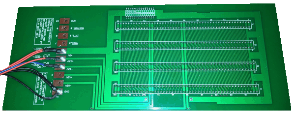
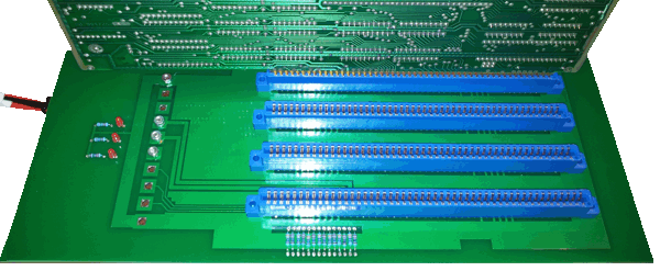
) (click on image for larger photo) |
This is a TM 990/102 extended memory CPU module. The module uses a 3 MHz TMS 9900 processor, has 128K bytes of on-board dynamic RAM and supports up to 16K bytes of EPROM. Memory can be expanded off-board up to 1M byte. The 40-pin IC bottom left is a TMS 9901 programmable systems interface chip, the centre 40-pin IC is a 74LS610 memory mapper (expands the 16-bit address bus to 20 bits), and the 40-pin IC on the right is a TMS 4500 dynamic RAM refresh controller. The module has a single serial I/O port. This module was listed on the eBay store Microwavetechnology in June 2011. |
) (click on image for larger photo) |
This is a TM 990/180M module. This module uses a 2.5 MHz TMS 9980 processor, which supports up to 16K bytes of memory. Up to 4K bytes of EPROM and 1K byte of RAM can be fitted on-board. This module was listed on the eBay store Vintage Processors in June 2011. |
) ) (click on images for larger photos) |
This is a TM 990/100MB module. It is similar to the TM 990/100MA module with the prototyping area but supports up to 8K byte RAMs and EPROMs. This module was listed on the eBay store Moses B Glick LLC in June 2016. |
) (click on image for larger photo) |
This is a TM 990/202 memory expansion module. The module is user-configurable and features two banks of eight sockets each, and can be fitted with various combinations of 4016 (2K × 8) static RAMs or 2516 (2K × 8), 2532 (4K × 8) or 2564 (8K × 8) EPROMs. The module supports 16- or 20-bit host-memory addressing and configurable wait states. This module was listed on the eBay store expertsurplus in November 2019. |
) (click on image for larger photo) |
This is a TM 990/203A memory expansion module that provides 64K bytes of TMS 4116 dynamic RAM. The module decodes both 16- and 20-bit addresses, with the upper and lower boundaries being selectable by DIP switches on 4K byte boundaries. The module can be configured to generate an interrupt in the event of a parity error. The interrupt is cleared by writing to a configurable CRU address. The DRAM refresh can be configured to transparent mode or cycle steal mode through a jumper. This module was listed on the eBay store Microwavetechnology in June 2011. |
) (click on image for larger photo) |
This is a TM 990/204 memory expansion module that provides 16K bytes of battery-backed CMOS RAM. The module includes a write protect switch and configurable wait states. This module was listed on the eBay store expertsurplus in November 2019. |
) (click on image for larger photo) |
This is a TM 990/303B floppy disk controller module. It supports up to four 8 1/2" or three 5 1/4" drives, single-sided only, single or double density. The controller module is intelligent, having its own on-board TMS 9900 processor, with a direct memory access (DMA) interface to the host bus. It supports 20-bit host-memory addressing and stores and retrieves data using high-speed DMA transfers. Controller firmware is in the on-board EPROMs, and includes the features: controller self test, read and write to/from diskette and host memory, bootstrap load from diskette software, format diskette, execute program in controller memory, and read status of specified drive. This module was listed on the eBay store expertsurplus in November 2019. Siemens also made a version of this module (Siemens continued the TM 990 range of modules after Texas Instruments discontinued them). |
) (click on image for larger photo) |
This is a TM 990/310 parallel input/output module. The module has 48 I/O bits, individually programmable as inputs or outputs, implemented through three TMS 9901 programmable systems interface chips. 27 of the bits may be programmed as interrupt inputs rather than inputs or outputs, with the interrupt priority encoding scheme permitting the module to be used as an interrupt expander for a processor module. The CRU base address is switch-selectable. This module was listed on the eBay store Pneumatplus in June 2011. |
) (click on image for larger photo) |
This is a TM 990/311 parallel input/output module. The module has 48 I/O bits, organised into 8-bit blocks. Each block is programmable as input or output. Two blocks make up a port, and each port has its own unique switch-selectable CRU base address. This module was listed on the eBay store Microwavetechnology in June 2011. |
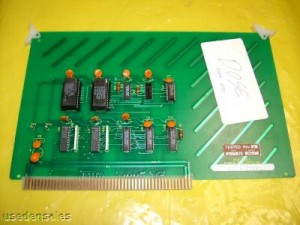 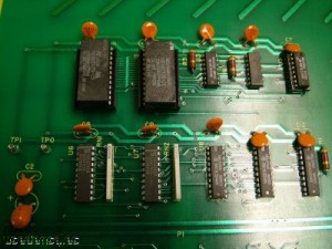 |
These two pictures are of a TM 990 Power Fail and Real-Time Clock (RTC) module used in Varian semiconductor manufacturing equipment, which used a number of TM 990 modules. Not sure if this module is manufactured by TI or a third party. This module was listed on the eBay store Semiconductor Equipment Spares in May 2008. |
) ) (click on images for larger photos) |
These are TM 990 64K byte and 512K byte bubble memory modules made by Fujitsu. These are from systems used in the early 1980's by a German textile machinery manufacturer. |
) (click on image for larger photo) |
This is a replacement CPU module made by MEN Mikro Elektronik GmbH of Nuremberg, Germany. This was used by the same machinery manufacturer as the two bubble memory modules above. The module has four serials ports and a RTC/calendar, as well as the obvious sockets for RAM and ROM. |
) (click on image for larger photo) |
RAM, ROM and twin serial port TM 990 board by Thermco Systems, who make semiconductor manufacturing equipment. Several of these modules were listed on the eBay store 602systech437az010021 in July 2016. |
) (click on image for larger photo) |
This is a copy made by Varian Associates, Inc. of a TI TM 990/101MB module, and is used in their Varian 120/160/180 XP ion implanter equipment. The module is nearly identical to the TI version, but has an additional 74LS00 at the top left of the PCB, presumably to replace the modification they had to make to TI's version of the board (a couple of tracks cut and jumper wires soldered on) to incorporate the Timekeeper RAM into the processor memory map. There is also an additional 3-pin jumper next to the TMS 9901. All the ICs on the PCB are socketed. This module was listed on eBay by user radioman95125 in November 2016. |
) (click on image for larger photo) |
This is a TM 990/101MB-3 module fitted with a memory expansion board. The expansion board has the TI logo on it so it might be a TI original part. This module was listed on eBay by user gelogistics in September 2017. |
