TMS 99110 (or 99105) Breadboard or PCB System
![]() Description
Description
![]() Specification
Specification
![]() Parts List
Parts List
![]() Technical Description
Technical Description
![]() References
References
![]() EPROM Binary Images
EPROM Binary Images
![]() Connecting to the Serial Port
Connecting to the Serial Port
![]() Programming - TIBUG and EVMBUG System Monitors
Programming - TIBUG and EVMBUG System Monitors
![]() Programming - BASIC
Programming - BASIC
![]() Programming - Forth
Programming - Forth
![]() Benchmarks
Benchmarks
![]() Project - TMS 9901 Expansion and Interval Timer
Project - TMS 9901 Expansion and Interval Timer
![]() Project - IDE Interface
Project - IDE Interface
This TMS 99110 system project provides a similar, minimal system to my TMS 9995 breadboard project, but using the Texas Instruments third-generation TMS 99110A 16-bit microprocessor
(a TMS 99105A microprocessor can also be used). The microprocessor runs at a maximum clock speed of 6 MHz, and includes a macrostore feature that contains floating point instructions as part of the machine language instruction set.
The system can be built either on a breadboard, or on a PCB (contact me if you
want a PCB - I'll order them in small batches once a couple of people have
expressed an interest).
The microcomputer is designed to interface with a Terminal program running on a PC, and run a system monitor, BASIC interpreter and Forth interpreter from EPROM - note though that there is no facility to load or save programs on this simple system
except by downloading or uploading them over the serial interface.
Preprogrammed EPROMs are available for purchase for users who do not have the
facilities to program their own.
The breadboard system is easy to
modify, expand and experiment with as the user wishes. On the PCB, take-off
points are included for all the main signals (including the demultiplexed
address/data bus) to enable the system to be expanded off the board.
This web page provides the specification, circuit diagram and technical description of the system, and gives the results of simple benchmarks performed on the TMS 99110A microprocessor against various configurations of the earlier TMS 9900 and TMS 9995 processors.
The project requires the parts listed in the table below. Approximate (UK) costs are included. You should be able to get everything off eBay if you don't want to use a specialist supplier such as Digi-Key.
Capacitor voltages can be the specified value or greater.
All resistors are 0.25W - 0.6W, 6mm body length.
| Circuit Diagram Reference | Description | Approx. Cost (excl. delivery) |
| - | For the breadboard system, 3 pieces of solderless breadboard, each section approx. 175 × 65 mm (64 contact points (holes) long by 10 wide, 2 pairs of bus strips along each edge of the board, see this photo) | £10 for the 3 sections |
| - | For the PCB version, contact me for availability of a PCB | - |
| U1 | TMS 99110A microprocessor (a TMS 99105A is normally easier to obtain) |
£30 (I got a working TMS 99105A from eBay seller "polida2008") |
| U2, U3 | 74ALS573 (BN or CN suffix OK) octal D-type transparent latch IC | £4 each |
| U4, U5 | 74ALS645 (AN or A-1N suffix OK) octal bus transceiver IC | £2 each |
| U6 | 74LS32 quad 2 input OR gate IC | £1 |
| U7 | 74LS04 hex inverter IC | £1 |
| U8, U9 | 32K byte 27256 or 27C256 EPROM, 120ns or faster (ST part # M27C256B-12XF1 works) | £2 each |
| U10, U11 | 32K byte 62256 static RAM, 85ns or faster, 'skinny' 0.3" wide package (Winbond part # W24257AK-20 or UMC part # UM61256K-15 work) | £2 each |
| U12 | 74LS138 3-to-8 line decoder IC | £1 |
| U13 | TMS 9902ANL asynchronous communications controller (ought to be the TMS 9902ANL-40 variant to work at 4 MHz, but a standard version seems to work OK) | £10 (ignore the overpriced ones at £140!) |
| U14 | MAX232CPE+ dual RS-232 transceiver | £2 |
| X1 | 16 MHz crystal (AEL Crystals part # X16M000000L259 should work) | £4 |
| C1, C2 | 5pF (or 4.7pF) ceramic capacitor | £0.20 for the 2 |
| C3, C5 - C10, C12 - C17 | 0.1μF ceramic decoupling capacitor | £1.30 for the 13 |
| C4 | 4.7μF tantalum capacitor, 16V | £0.30 |
| C11 | 22μF electrolytic capacitor, 16V | £0.30 |
| C18 - C22 | 1μF electrolytic capacitor, 16V | £1.75 for the 5 |
| R1 - R6 (plus R8 - R11 on PCB V3 and later) |
10K metal film 0.6W resistor | £0.60 for the 6 |
| R7 | 220 Ohm metal film 0.6W resistor | £0.10 |
| D1 | LED, 3mm, red | £0.20 |
| SW1 | Single pole, push-to-make, PCB mount, non locking switch | £1.50 |
| J1 | DC power socket (female), 5.5 × 2.1mm, PCB mount if building on the PCB | £1 |
| J2 | 9-way D-type socket (female), PCB mount if building on the PCB | £2 |
| - | IC sockets if building on the PCB (all 0.1"
pin spacing): • 1 × 40 pin • 4 × 28 pin, 0.6" wide • 2 × 28 pin, 0.3" wide • 4 × 20 pin • 1 × 18 pin • 2 × 16 pin • 2 × 14 pin |
£5 |
A circuit diagram for the project is available here (PCB V1 and V2) and here (PCB V3), and a high resolution photograph of the breadboard system here and the PCB here (a few small updates have been made to the circuit diagram since the photographs were taken, should you be looking at them closely). The following description should be read in conjunction with the component datasheets, links to which are given in the References section below.
Processor U1 derives its clock from crystal X1. The crystal frequency is internally divided by 4 to give the processor clock speed. The processor clock also drives the TMS 9902 that provides the serial port. The standard TMS 9902 device operates with a clock speed of 3 MHz which requires a 12 MHz crystal. If a TMS 9902-40 device is obtained, this will operate at up to 4 MHz which requires a 16 MHz crystal†. The processor and memory interface have been tested at the maximum processor clock speed of 6 MHz which requires a 24 MHz crystal, although at this speed the
TMS 9902 will not work so the system provides no external connectivity, so has
little practical use.
†
A couple of standard TMS 9902s have been tested at 4 MHz and were found to work
fine as well.
The following processor inputs are pulled high by resistors R1 - R5:
The processor /RESET input is normally pulled high by resistor R6. To reset the processor, switch SW1 is pushed to pull the /RESET input low. Capacitor C4 provides a 'power-on reset' function.
Interrupt code inputs IC0 - IC3 are configured by pull-up/down resistors R8 - R11 to interrupt level 1.
The processor has a 16-bit multiplexed address and data bus. At the start of each memory cycle, the processor places the address on the multiplexed bus with the ALATCH output high, then takes ALATCH low which latches the address in octal D-type transparent latches U2 and U3. The multiplexed bus is interfaced to the memory data bus through octal bus transceivers U4 and U5. The bus transceivers are only enabled during memory cycles (the processor /MEM output is active low), whereas the address latches are permanently enabled as the address bus is also used during CRU input/output cycles. The direction of data flow through the bus transceivers is controlled by the processor /RD output.
EPROMs U8, U9 and static RAMs U10, U11 are connected to the demultiplexed processor address and data buses. Note that at the time Texas Instruments labelled their address and data bus lines the opposite way round to the rest of the industry, so the low numbered processor address and data bus lines are connected to the high numbered EPROM and RAM address and data bus lines, and the high numbered processor lines are connected to the low numbered EPROM and RAM lines. The EPROM and RAM /OE (Output Enable) inputs are connected to the processor /RD output, which when active low indicates that the processor has disabled its data bus output buffers to allow external memory to output data (via the bus transceivers) onto the data bus. The EPROM /CE (Chip Enable) input is derived by ORing address bus line A0 with the processor /MEM (Memory Enable) output, such that the EPROM is enabled during memory cycles in the address range >0000 - >7FFF. The RAM /CE input is derived in a similar way by inverting address bus line A0 and ORing it with /MEM such that RAM is enabled during memory cycles in the address range >8000 - >FFFF.
The processor /PSEL (page select) output, which forms a 17th address bit and is derived from bit 8 of the status register, is also latched by U2, then inverted and applied to the MS address bit of the EPROMs and RAMs to divide each into two pages. Inverting /PSEL means that default operation (following a reset) takes place in the lower half (first page) of each device, which makes it easier to program the EPROMs.
The pair of RAMs have been fitted to the breadboard in a piggyback fashion to reduce the wiring involved in connecting them, while the EPROMs have been fitted in ZIF sockets to make them easy to replace.
3-to-8 line decoder U12 decodes address bus lines A7, A8 and A9 during CRU input/output cycles when /MEM is high to provide chip enable signals for 8 blocks of 32 bits of CRU address space. Output /Y0 is active low when addressing CRU bits 0 - 31, /Y1 is active when addressing bits 32 - 63, and so on.
TMS 9902 Asynchronous Communications Controller (ACC) U13 is a CRU peripheral device which provides the interface between the processor and a serial, asynchronous, RS-232 communications channel. The connection to address decoder U12 maps the device to processor CRU address bits 0 - 31. RS-232 driver/receiver U14 generates ±10V supplies from the single +5V supply and provides signal level conversion between RS-232 signal levels (±3V to ±25V) and the TTL signal levels used by U13. A simple 3-wire RS-232 interface is implemented through connector J2.
The circuit requires a single +5V regulated supply, which is input through connector J1. Capacitor C11 provides power supply smoothing. LED D1 provide a 'power on' indication, with resistor R7 limiting the current through the LED. The supply to individual ICs is decoupled by capacitors C3, C5 - C10, and C12 - C17.
At a processor clock speed of 3 MHz, memory access time is 210ns (minus decoding logic delay). At 6 MHz, this reduces to 85ns. The RAMs used in the system are a pair of Winbond 32K × 8 W24257A CMOS static RAMs with an access time of 20ns; these are clearly fast enough at all supported clock speeds (UMC RAM type UM61256K-15 is also confirmed as compatible). The EPROMs used are a pair of ST 32K × 8 M27C256 CMOS devices with an access time of 120ns; these were found to work even at a 6 MHz clock speed - the rated access times are presumably for worst case conditions across the full operating temperature range.
TMS 99110A processor data manual
The 99000 Microprocessor - Architecture Software and Interface Techniques book [120 MB download]
ST M27256 EPROM data sheet
Winbond W24257A static RAM data sheet
74ALS573 octal D-type transparent latch data sheet
74ALS645 octal bus transceiverdata sheet
74LS04 hex inverter IC data sheet
74LS32 quad 2 input OR gate IC data sheet
MAX232CPE dual RS-232 transceiver data sheet
TMS 9902ANL asynchronous communications controller data sheet
74LS138 3-to-8 line decoder IC data sheet
System monitor. The project uses a modified version of either the TIBUG system monitor from TI's TM 990 range of microcomputer modules, or the EVMBUG system monitor from TI's TMS 9995 Evaluation Module. TIBUG and EVMBUG are described on this page.
The BASIC interpreter is based on a port of the Powertran Cortex Power BASIC made for my TM 990 computer. The Cortex BASIC user guide is available here.
The Forth interpreter is based on fig-FORTH 9900 Release 1.0 (March 1981). Details on fig-FORTH are available at www.forth.org.
Each link below is to a zip file which contains two EPROM images - one image for the even (most significant) byte, and one for the odd (least significant) byte. Which EPROM goes in which socket is clearly marked on the PCB.
Link to TIBUG system monitor EPROM image here.
Link to EVMBUG system monitor and BASIC EPROM image here (BASIC runs from RAM).
Link to EVMBUG system monitor and BASIC EPROM image here (BASIC runs from EPROM).
Link to EVMBUG system monitor and Forth EPROM image here.
A Terminal program running on a PC is required to communicate with the system. Configure the terminal for 19200 Baud, 7 data bits, even parity, 2 stop bits.
To connect the system to a 9-pin serial port on a PC, a serial cable with male and female connectors is required, with the following pins connected (as a minimum): 2‑2, 3‑3, 5‑5. If using a serial-USB adaptor, the serial port should connect to the system directly.
The TIBUG and EVMBUG system monitors provide an interactive interface between the user and the system. They are described on this page.
If you are new to programming a single board computer of this type, the user manual for the TM 990/100M microcomputer (which is based on the earlier TMS 9900 processor) provides a good introduction to the processor architecture and concepts.
The BASIC interpreter is based on a port of the Powertran Cortex Power BASIC made for my TM 990 computer. BASIC is programmed in the EPROM along with a slightly modified version of the EVMBUG monitor.
Two versions of BASIC are available (in different EPROM images):
When the system is reset, a menu is displayed: press 1 to run the EVMBUG monitor, or press 2 to run BASIC.
TMS 99110 PCB SYSTEM
BY STUART CONNER
PRESS 1 FOR EVMBUG MONITOR
PRESS 2 FOR CORTEX BASIC
(Press 2)
-- TMS 9995 Breadboard BASIC Rev. 1.1 --
[Ported from Cortex BASIC (C)1982 by Stuart Conner]
*Ready
The Cortex BASIC user guide is available here.
Mapping between the keys on the Cortex computer and the keys on the PC keyboard is as shown in the following table.
| Cortex Key | PC Keyboard Key |
| Enter | Return |
| Edit | Ctrl-T |
| Clear | Ctrl-L |
| Escape | Esc |
| Graphic | (not supported) |
| Insert | Ctrl-V |
| Delete | Ctrl-C |
| Rubout | Backspace |
| Cursor Up | Ctrl-E |
| Cursor Down | Ctrl-X |
| Cursor Left | Ctrl-S |
| Cursor Right | Ctrl-D |
| Home | Ctrl-H |
The version of EVMBUG supplied with BASIC is modified such that the automatic delay functionality after printing each line on a mechanical teletype is disabled. This won't make any difference unless you happen to be using a mechanical teletype ...
When BASIC is in use, all input is automatically converted to upper case.
There are some changes and restrictions in the TMS 99110 implementation as compared to the implementation described in the Cortex user guide:
The Forth interpreter is based on the fig-FORTH 9900 Release 1.0 (March 1981). The source code is available here (the TMS 99110 implementation is slightly modified in terms of the memory pointers used and the input/output routines). Forth is programmed in the EPROM along with a slightly modified version of the EVMBUG monitor. When the system is reset, a menu is displayed: press 1 to run the EVMBUG monitor, or press 2 to run Forth.
TMS 99110 PCB SYSTEM
BY STUART CONNER
PRESS 1 FOR EVMBUG MONITOR
PRESS 2 FOR FIG-FORTH
(Press 2)
9900 fig-FORTH Rel 1.0
The Forth code is copied from EPROM to RAM and then run from RAM when it is selected at the menu. All input and output is over the RS-232 interface, and there is no means of loading or saving a program.
Various Forth tutorials are available here. Note that different versions of Forth support slightly different dictionaries so you might find some examples in the tutorials that will not work on the TMS 99110 implementation.
The version of EVMBUG supplied with Forth is modified such that the automatic delay functionality after printing each line on a mechanical teletype is disabled. This won't make any difference unless you happen to be using a mechanical teletype ...
The following benchmarks give the results of simple tests performed on the TMS 99110A microprocessor against various configurations of the earlier TMS 9900 and TMS 9995 processors.
TMS 9900:
TMS 9995:
TMS 99110:
Testing of the 9900 was performed on my TM 990 system, the 9995 on my 9995 breadboard system, and the 99110 on this 99110 breadboard system. Timings were made using a simple stop watch.
The program copies from EPROM to RAM a routine that loops through a NOP instruction 10 × >FFFF times, then reads a word from EPROM 10 × >FFFF times, then repeats. This generates blocks of pulses on the EPROM /CE line that can be easily seen with a logic probe.
Note: Slight changes were made to the program below for the TMS 9995 tests to locate the code and workspace in the appropriate places in memory.
AORG >0000 Assemble at the bottom of EPROM.
WS EQU >8000 Workspace in RAM.
RESET DATA WS Reset workspace vector.
DATA START Reset code start vector.
* (other interrupt vectors not used)
*Loop routine to be copied to RAM.
CODE LI R1,10 Outer loop count.
LOOP1 SETO R0 Inner loop count of >FFFF.
LOOP2 NOP Do nothing.
DEC R0 Decrement inner loop count.
JNE LOOP2 Loop round.
DEC R1 Decrement outer loop count.
JNE LOOP1 Loop round.
LI R1,10 Outer loop count.
LOOP3 SETO R0 Inner loop count of >FFFF.
LOOP4 MOV @>0000,R2 Copy data from EPROM (and ignore it).
DEC R0 Decrement inner loop count.
JNE LOOP4 Loop round.
DEC R1 Decrement outer loop count.
JNE LOOP3 Loop round.
B @WS+32 Repeat endlessly.
CLEN EQU $-CODE
*Routine to copy loop routine from EPROM to RAM.
START LI R1,WS+32 Where to copy the code to (RAM after the workspace).
LI R2,CODE Start address of code to copy.
LI R3,CLEN Length of code to copy.
COPY MOV *R2+,*R1+ Copy code.
DECT R3
JH COPY
B @WS+32 Jump to code.
END
| Processor / Configuration | Timing | Time Per Cycle |
| TMS 9900, 3 MHz, no wait states | 4 cycles in 64 seconds | 16.0 seconds per cycle |
| TMS 9995, 3 MHz, with code and workspace in internal 256 byte (16-bit, no wait states) memory | 13 cycles in 62 seconds | 4.8 seconds per cycle |
| TMS 9995, 3 MHz, with code and workspace in external memory with no wait states | 9 cycles in 63 seconds | 7.0 seconds per cycle |
| TMS 9995, 3 MHz, with code and workspace in external memory with single wait state | 5 cycles in 64 seconds | 12.8 seconds per cycle |
| TMS 99110, 3 MHz, no wait states | 15 cycles in 62 seconds | 4.1 seconds per cycle |
| TMS 99110, 4 MHz, no wait states | 20 cycles in 62 seconds | 3.1 seconds per cycle |
| TMS 99110, 5 MHz, no wait states | 24 cycles in 60 seconds | 2.5 seconds per cycle |
| TMS 99110, 6 MHz, no wait states | 29 cycles in 60 seconds | 2.0 seconds per cycle |
Test program 2 is a BASIC program that runs under a port of the Powertran Cortex Power BASIC programmed into EPROM and copied and run from RAM. The program draws the graph shown below the listing ... or at least it does if a VDP is included in the test system, but the absence of a VDP does not alter the program timing.
10 GRAPH : XS=2: YS=2
20 A=256: B=A*A: C=192
30 FOR X=0 TO A STEP XS: S=X*X: P=SQR[B-S]
40 FOR I=-P TO P STEP 6*YS
50 R=SQR[S+I*I]/A
60 Q=(R-1)*SIN[10*R]
70 Y=INT[I/3+Q*C]
80 IF I=-P THEN M=Y: N=Y
90 IF Y>M THEN M=Y
100 IF Y<N THEN N=Y
110 IF (M=Y OR N=Y) THEN X1=X/2: Y1=100-Y/2: PLOT 128+X1,Y1: PLOT 128-X1,Y1
120 NEXT I
130 NEXT X
140 TEXT
150 PRINT "** FINISHED**"
| Processor / Configuration | Program Run Time |
| TMS 9900, 3 MHz, no wait states | 320 seconds (5’ 20’’) |
| TMS 9995, 3 MHz, with code and workspace in external memory with no wait states | 166 seconds (2’ 46’’) |
| TMS 9995, 3 MHz, with code and workspace in external memory with single wait state | 285 seconds (4’ 45’’) |
| TMS 99110, 3 MHz, no wait states | 105 seconds (1’ 45’) |
| TMS 99110, 4 MHz, no wait states | 77 seconds (1’ 17’’) |
Adding a TMS 9901 to the system and using its interval timer is fairly straightfoward. The device specifically has to be a TMS 9901-40 to match the 4 MHz clock speed of the processor (assuming a 16 MHz crystal is used).
A circuit diagram of the expansion is available here. Only a TMS 9901-40 and some wire are required. A copy of the TMS 9901 datasheet is available here.
The TMS 9901 is fitted across the two spare IC sockets on the PCB as shown here. Note the specific placement of the TMS 9901 in the sockets which positions pins that don't need connections between the two sockets. Note also that the four PCB tracks connecting IC0 - IC3 to GND have to be cut with a sharp craft knife as shown. (On PCB V3 and later, a spare 40-pin IC socket is included, and IC0 - IC3 are connected to the power rails through pull-up/down resistors so no tracks have to be cut.)
A photo showing the wiring connections to the TMS 9901 is available here. Use this in conjunction with the circuit diagram above to ensure you make the connections correctly. You might want to fit the TMS 9901, then connect the wires in the order listed below and verify that the board still works after connecting each group of wires. This makes it easier to diagnose any problems if the board stops working.
Example code to use the interval timer on the TMS 9901 to print a character to the terminal every 2 seconds is listed below. The code has to be assembled then the object code loaded using the EVMBUG monitor. When the code is run (use the EVMBUG IR command to set the program counter (PC) to 8000 then the EX command to run it), it programs the TMS 9901 then returns to the EVMBUG prompt. The interval timer generates interrupts that are processed in the background while you carry on using EVMBUG, and the interrupt service routine prints a character every 2 seconds that will be mixed in with whatever text output EVMBUG is producing at the time.
*Set the interval timer on the TMS9901 to generate an interrupt every 250ms,
*and use this to print a character to the terminal every 2 seconds.
AORG >8000 Assemble at the bottom of RAM.
LWPI WS Set workspace.
*The TMS9901 timer generates a level 3 interrupt. The WP and PC for this
*interrupt are defined in EVMBUG as >F0BE and >F0DE. Store a Branch instruction
*at the PC vector to jump to code further below.
LI R1,>0460 Op-code for Branch instruction.
MOV R1,@>F0DE
LI R1,INTRPT
MOV R1,@>F0DE+2
*Clear the counter used to count the 250ms interrupts.
CLR @INTCNT
*Program the TMS9901 timer. With a 4 MHz crystal, one clock 'tick' is 0.016ms,
*so need to program the timer with a value of 15,625 for an interval of 250ms.
LI R12,>0040 CRU base address for the TMS9901.
LDCR @CLKVAL,15 First bit sets Control bit to 1 to select clock mode,
* then remaining bits are the clock register value.
*Enable level 3 interrupts on the TMS9901 and TMS9900.
SBZ 0 Set Control bit to 0 to select interrupt mode.
SBO 3 Enable (unmask) the level 3 interrupt.
LIMI 3 Enable processor interrupt levels 0 - 3.
*Return to EVMBUG.
B @>0080 Quit back to EVMBUG.
***THIS IS THE SECTION OF CODE CALLED AT EACH INTERRUPT***
*Clear the TMS9901 timer interrupt.
INTRPT LI R12,>0040 CRU base address for the TMS9901.
SBO 3 Clear the level 3 interrupt.
*Increment the interrupt counter and check if 2 seconds has elapsed.
*Return from interrupt if not.
INC @INTCNT
C @INTCNT,@D08 8 interrupts counted?
JNE EXIT
*2 seconds has elapsed. Print a character. Can't use an XOP in the
*interrupt routine to program the TMS9902 directly.
CLR @INTCNT Clear the interrupt counter.
CLR R12 CRU base address for the TMS9902.
SBO 16 Set /RTS on.
WENTRY1 TB 22 Transmit buffer register empty?
JNE WENTRY1 No, loop until it is.
LDCR @CHAR,8 Send character.
WLOOP1 TB 22 Transmit buffer register empty?
JNE WLOOP1 No, loop until it is.
EXIT RTWP Return from interrupt.
*Workspace and data.
WS BSS 32 Workspace.
INTCNT DATA 0 Interrupt counter.
CLKVAL DATA >7A13 Clock register value of 15,625, shifted one bit
* left, then '1' added for Control bit.
D08 DATA 8
CHAR TEXT 'A' Character to print.
END
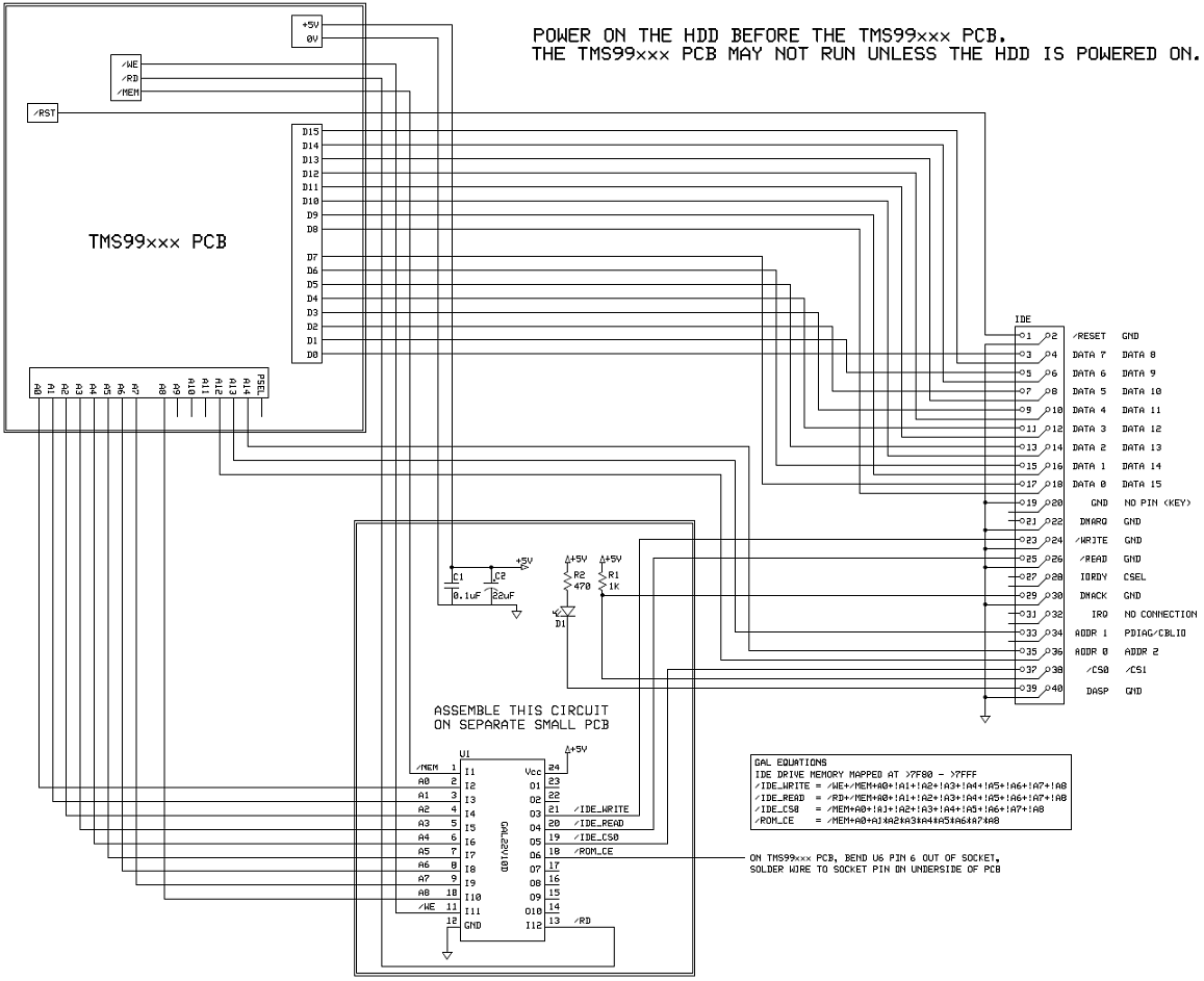
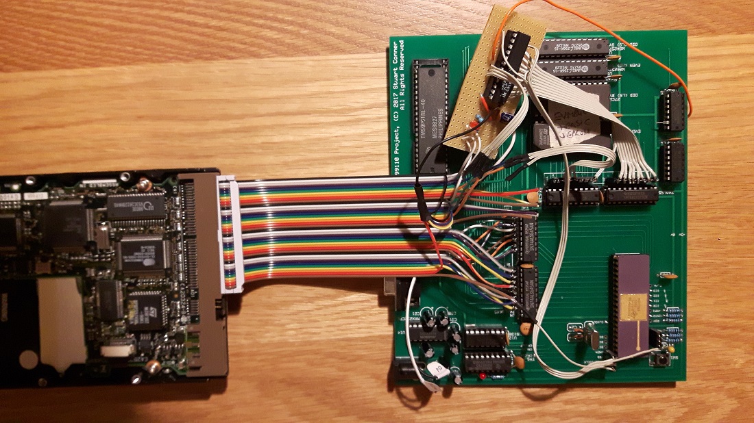
The schematic and photo below shows an IDE interface for the TMS 99110 PCB. It needs one soldered connection to the PCB but otherwise all the connections are to the pin strips already designed into the PCB. The circuit uses a GAL for the address decoding, with the interface memory mapped to >7F80 - >7FFF. Tested using tweaked IDE software that I wrote for my TM 990 IDE board.