and Disassembler Cartridge
Honoured to receive the Rob Tempelmans Plat award in 2013
and an Edgar Mauk Award in 2018
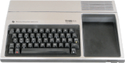
TI-99/4A Computer
The Texas Instruments TI-99/4A was an early home computer, released in June of 1981. The computer holds the distinction of being the first 16-bit personal computer, having a 16-bit TMS 9900 CPU running at 3.0 MHz.
 |
For a full description of the system, see this comprehensive Wikipedia entry. |  |
This is a port of the 'Power BASIC' interpreter used with the TMS9995-based Powertran Cortex machine. Features and constraints are as follows:
Code for direct control of the RS-232 and parallel port hardware (bypassing use of the DSRs) is also available, but including this will obviously reduce the amount of RAM available for program storage.
Various download options are available, depending on how you intend to run the program. For each option, there is also the choice of whether to download the 40-column or 80-column text version. Download links are in the table below, with a description of the various options below that.
| Text Version | Disk Image | 32K EPROM Image, Inverted Bank Switching |
32K EPROM Image, Non-Inverted Bank Switching |
512K EPROM Image, Non-Inverted Bank Switching |
| 40-column | Cortex BASIC 40 v1_7.zip |
Cortex BASIC 40 32K Inverted v1_7.zip |
Cortex BASIC 40 32K Non-Inverted v1_7.zip |
Cortex BASIC 40 512K Non-Inverted v1_7.zip |
| 80-column (requires F18A) |
Cortex BASIC 80 v1_7.zip |
Cortex BASIC 80 32K Inverted v1_7.zip |
Cortex BASIC 80 32K Non-Inverted v1_7.zip |
Cortex BASIC 80 512K Non-Inverted v1_7.zip |
The program is on a TiDisk format image and named "CBASIC". This disk image format works with all the simulators listed above (F18A support needed for the 80-column version) and with the CF7+/NanoPEB device on real hardware. To run the program, boot with the Editor Assembler cartridge, select E/A option 3 and type the filename DSKn.CBASIC. The program should load and display the *Ready prompt within a few seconds.
With the disk versions, the size of the code means that only about 5K of RAM is available for your program and variable storage. Programs are stored in a tokenised format so what free memory there is is used quite efficiently.
This is a binary image which can be used as follows:
With the bank-switched cartridge versions, some of the code is copied from the cartridge to RAM, and 8K is left running from the cartridge, so just over 14K of RAM is available for your program and variable storage.
This is a binary image which can be used as follows:
As with the 32K EPROM image version above, just over 14K of RAM is available for your program and variable storage.
This is a binary image which can be used as follows:
As with the 32K EPROM image versions, just over 14K of RAM is available for your program and variable storage.
The Cortex BASIC user guide is available which details the Cortex BASIC implementation. This document was recreated by Jim Fetzner from a poor quality photocopy.
| Cortex Key | Console Key | Classic99 (PC Keyboard) Key |
| Enter | ENTER | Return |
| Edit | CTRL-T | Ctrl-T |
| Clear | CTRL-L | Ctrl-L |
| Escape | FCTN-9 (BACK) | Esc or Alt-9 |
| Insert | FCTN-2 (INSERT) | Insert or Alt-2 |
| Delete | FCTN-1 (DELETE) | Delete or Alt-1 |
| Rubout | FCTN-3 (ERASE) | Alt-3 |
| Cursor Up | FCTN-E | Cursor Up |
| Cursor Down | FCTN-X | Cursor Down |
| Cursor Left | FCTN-S | Cursor Left |
| Cursor Right | FCTN-D | Cursor Right |
| Home | CTRL-H | Home |
Some sample program listings can be downloaded here. See the @Program Descriptions.txt file within the zip file for program descriptions.
All these programs were typed in or developed on my TM990 system but many will run on the TI-99/4A without modification. Those that interact with the hardware such as the SID chip will require modification to run on the TI-99/4A - I leave these for the reader to experiment with. You will have to work out a way to enter these listings on your system if you don't simply want to type them in (hint: if you're using the Classic99 simulator, copy the text listing to the clipboard then use the Edit > Paste command to 'type' them in).
Most of these programs will require you to use a cartridge version of Cortex BASIC (the 40-column version is probably best to match the original display) - there won't be enough RAM available if you use the disk version.
There are some changes and restrictions in the TI implementation as compared to the implementation described in the Cortex user guide. Note that some commands work differently to their familiar equivalents in TI BASIC. If you think you've found a bug in the interpreter code, download the Cortex emulator (written by David Hunter) and check your program on there. You can report any confirmed bugs to me at ti99(at)stuartconner(dot)me(dot)uk.
Revisions
1.0 - 29 Jan 2011 - Initial release.
1.1 - 10 Feb 2011 - Added load/save functionality.
1.2 - 17 Feb 2011 - Moved most processor workspaces to 16-bit 256-byte console RAM to increase speed.
1.3 - 01 Apr 2011 - Improved key handling with the KEY() function, which would previously miss some key strokes. To check for keys pressed in a game for example, call NOESC at the start of the program, then A=KEY(0) to check for a key press, and IF A=01BH THEN STOP as part of the key handling routine to enable <Escape>ing out of the program.
1.7 - 05 Dec 2015 - Refactored to enable code to build image for either E/A option 3 file or TI-99/4A bank-switched cartridge.
This is a disk version of the TI Invaders cartridge, created from an original
program listing. The game can be downloaded here (Invaders.zip,
V9T9/.tidisk format). The program name is INVADERS - load using Editor/Assembler option 3. The program auto-starts on loading.
The game controls are 'S' and 'D' to move left and right, and '.' to fire.
The program supports the cheat mode, which is accessed when on the title screen by pressing <Shift>838. This prompts for a Y/N to play slow speed then two digits for the number of the screen to start on. None of these inputs will be displayed, and it is not necessary to press <ENTER>.
| Disk: Miscellaneous.zip (V9T9/.tidisk format) | |
|
Programs with names in black are written/generated by me. Programs with names in red are copied from other sources. |
|
| CATALOG | BASIC disk catalogue program from TI disk drive manual. |
| CFMGR CFMGS |
Compact Flash Drive Volume Manager. E/A 5 format. |
| CONV_BASES | Subroutine (for MERGE-ing into other programs) to convert a binary, decimal or hexadecimal number to binary, decimal or hexadecimal. Lines numbered from 10000. |
| DISASSMBLR | TMS 9900 assembly language disassembler, running under TI Extended Basic with 32K RAM. |
| DISASS/S DISASS/O |
Source and object files for assembly language utility to print to the screen in text mode (40 characters × 24 lines). |
| MGR3 MGR4 |
DM-1000 (V3.5) Disk Manager (copied from Funnelweb). E/A 5 format. |
| CART_RAM/S CART_RAM/O |
Source and object files for assembly language program to save/load the contents of the SuperCart RAM (>6000 - >7FFF) or MiniMem RAM (>7000 - >7FFF) to/from a data file. Also has an option to fill the RAM with zeroes. Load using E/A option 3 (for the SuperCart) or MiniMem option 3, 1 (for the MiniMem). Program auto-starts on loading and detects the cartridge type. Requires 32K RAM expansion to be present. The following RAM image files can be loaded using the CART_RAM/O program: |
| SC_START | Data file containing the RAM image for the SuperCart startup menu. |
| MM_LBLA | Data file containing the RAM image for the MiniMem Line-By-Line Assembler (LBLA). Program names: OLD, NEW. |
| MM_LINES | Data file containing the RAM image for the MiniMem Lines demonstration program. Program name: LINES.
To load and run the MiniMem LBLA for example: |
| RD_REF_TBL | BASIC program to display the contents of the REF/DEF table when running with the Extended Basic, Editor/Assembler or MiniMem modules. |
| SYSTEX | XB/assembly language hybridisation program. Version 1.0, ©1985, Barry Boone. Allows you to save assembly language programs/utilities as part of XB program files. |
| XBOPT5 | E/A 5 format loader for Extended Basic. Version 3.1, 1987, Barry Boone. To use, make a copy of the program, then edit line 110 to specify the program to load. |
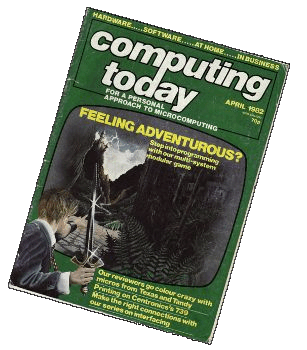
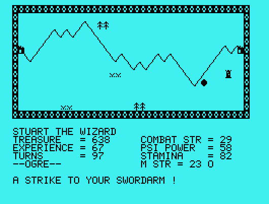
| "The Valley" was an adventure game published as a "type in" program listing in
the UK Computing Today magazine, April 1982. It was originally developed
for the Commodore PET but the "universal BASIC" listing enabled it to be
easily adapted to other micros of the time such as the Tandy TRS-80,
Oric and Sharp MZ-80K. You can read more about the history of the program
here and
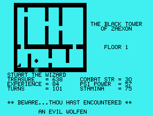
here. Choose your character type carefully ... Barbarians recover quickly but their magic doesn't come easily. A Wizard? Slow on the draw and slow to mature ... but live long enough and grow wise enough and your lightning bolts are almost unstoppable ... The Valley is a real-time game of adventure and survival. You may choose one of five character types to be your personal 'extension of self' to battle and pit your wits against a number of monsters. Find treasure, fight a Thunder-Lizard in the arid deserts of the Valley, conquer a Kraken in the lakes surrounding the dread Temples of Y'Nagioth, or cauterise a Wraith in the Black Tower. In fact, live out the fantasies you've only dared dream about. BUT BEWARE ... more die than live to tell the tale! |
 |
A version of the game to run on the TI-99/4A can be downloaded
here (The_Valley.zip, V9T9/.tidisk
format). The program requires XB and 32K memory.
To run the program, load and run the file RUN
(OLD DSK.THE_VALLEY.RUN).
Program developed and tested on a console with 32K × 16 bit RAM and CF7+ Compact Flash Drive. Tested on the Win994a simulator.

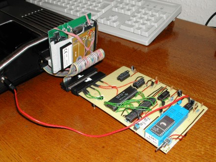
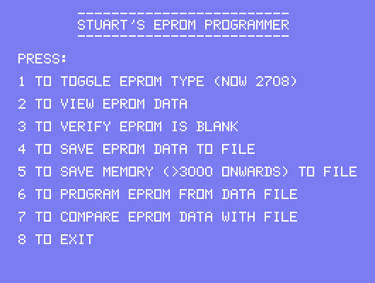
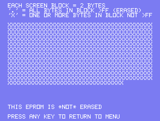
| This project is an EPROM Programmer to read and program TMS 2708 (1K × 8) and TMS 2716 (2K × 8) EPROMs Note 1. It was developed to program EPROMs for my TM 990 system. The circuit is based around a TMS 9901 Programmable Systems Interface IC which is used to apply address, data and control signals to the EPROM. A control program, written in assembly language, enables the user to view the data on an EPROM as both hex and ASCII, to verify that an EPROM is blank, to save the data from an EPROM to a data file, to save an EPROM image in memory to a data file, to program an EPROM from a data file, and to compare the data on an EPROM with a data file. The board is designed to plug into the TI-99/4A console side port via a Y-cable (side port splitter), which allows the PEB or other storage device to also be connected at the same time Note 2. The board requires a +12V supply, which can be provided by fitting a DC power socket to the side of the console, wired directly to the +12V supply from the internal power supply board. A circuit diagram of the EPROM Programmer is available here. The object code for the control program Note 3 is available here (disk in V9T9 format; load program EPROM/O using Editor/Assembler option 3). Screenshots of the control program in use are shown below - click each for a larger image. |
 |
Note 1: Texas Instruments TMS 2716 EPROMs have a different pinout and programming requirements from 2716 EPROMs from other manufacturers. The board is compatible with TMS 2716 EPROMs from Texas Instruments only.
Note 2: The board and software have been developed using a TI-99/4A with a CF7+ Compact Flash Drive for program storage. It has not been tested with a PEB attached, but there is no reason why it should not work. Note also that I found the CF7+ Compact Flash Drive a bit temperamental connected to the Y-cable as supplied. I ended up shortening the 'arm' of the cable that the CF7+ was connected to, and it then worked perfectly. Positioning the two arms of the Y-cable at 90° to each other may also be sufficient for reliable operation.
Note 3: The algorithm to program an EPROM contains some timing loops which control the application of the +26V programming pulses. The object code compiled here is for a TI-99/4A with 32Kbyte RAM on the internal 16-bit data bus. If the program is to be used on a console with external 32Kbyte RAM (on a CF7+ or in the PEB for example), these programming pulses will be extended (as the console is running slower), but an EPROM will probably still program reliably.
| This CF To Disk Transfer Utility helps you copy disk volumes between a CF card and your hard drive. It is in essence a graphical front end to the cf2dsk.exe and dsk2cf.exe programs supplied with the TI-99/4A Compact Flash Drive. Full details are available in this readme file (including how to run the utility and the cf2dsk.exe and dsk2cf.exe programs under Windows 7). (The files originally provided with the CF7+ drive can be downloaded here or from the designer's website.) |
 |
The console motherboard, fitted with the TI Extended BASIC cartridge, draws the following current from the power supply board:
On the 'standard' power supply board, the +5V regulator is a switched mode design, and the +12V and -5V regulators are of the linear type.
The NanoPEB draws from the +5V supply ~75mA 'at rest', rising to ~85mA when accessing the CF card .
This modification adds 32K RAM to the console, internally on the 16-bit data bus. The RAM occupies the same address ranges as the 32K RAM expansion card normally fitted in the Peripheral Expansion Unit: >2000 - >3FFF and >A000 - >FFFF. The modification disables the wait state generation circuit when the RAM is accessed, making it faster than the RAM in the external 32K RAM expansion card.
The circuit diagram for the modification is shown below. The circuit diagram shows the original console components and connections in grey, with the modifications shown in black. A photo of the completed modification is shown below the circuit diagram.
The modification uses two 128Kbyte CMOS RAMs (NEC type UPD431000ACZ-70, equivalent parts should work). 24 pins of these 32 pin devices are largely pin-for-pin compatible with the existing console ROMs U610 and U611, which makes it easy to piggy-back them on the ROMs with the non-compatible pins and the extra pins bent out and wired individually. The extra address lines and the /WE signal are taken directly from the processor.
Existing 3-to-8 line decoder U504 provides convenient address decoding for the address space to be occupied by the RAM. A quad AND 74LS08 device is used to combine the chip select lines to drive the RAM /CS and /OE lines. A switch (fitted on the console back panel) and 1K pull up resistor on these lines enables the RAM expansion to be disabled, if required. The 74LS08 device is piggy-backed on another 14 pin LS device on the board for the +5V and GND supplies, with the other pins wired individually.
The existing console ROMs and scratchpad RAMs are fitted on the 16-bit data bus, and the existing circuit which includes NAND gate U606 pins 11/12/13 is used to disable the wait state generation circuit when the ROMs or scratchpad RAMs are accessed (wait states are introduced for all memory accessed through the console 16-to-8 bit data multiplexer). The same circuit is used to disable the wait states for the 32K expansion RAM by ANDing the ROM chip select with the RAM chip select, and feeding this to U606/13. This pin is physically cut to isolate it from the ROM chip select routed through the board (alternatively, the relevant trace on the board could be identified and cut), and the new ROM/RAM chip select wired to it.
(Ignore the grey cable on the left - that's a reset switch)
The Line-By-Line Assembler (LBLA) provided on cassette tape with the TI-99/4A Mini Memory module contains a bug, whereby if assembling instructions with two symbolic addressing operands (for example MOV @L1,@L2), and both operands are unresolved references (that is, L1 and L2 in the previous example have not yet been defined), the first instruction will be assembled correctly, but further instructions will not as the label for the second operand is not added to the symbol table, and hence is not 'filled in' when the label is defined later.
The bug is in a small loop starting at address >7248 that clears memory addresses >7194 - >719F after assembling each instruction. This loop also needs to clear one extra word (address >71A0) as this word is used when assembling an instruction to record whether the second operand is an unresolved symbolic reference or not. The bug can be fixed by simply increasing the loop counter by 1, as follows:
A .wav file of the LBLA cassette can be downloaded here.
| This is a simple cartridge which contains a copy of the Mini Memory
Line-By-Line Assembler (LBLA), TIBUG monitor (which is similar to the Mini Memory
EASY BUG and the Editor/Assembler Debugger program), and a disassembler. The cartridge is 8K and works with a 27(C)64 EPROM on a 64K/128K ROM cartridge board. The EPROM image can be downloaded here. 32K RAM expansion is required to use the cartridge. The programs in the cartridge use the memory block >2680 to approximately >2840 in the low memory area, so avoid assembling any programs at these memory locations. With the cartridge inserted, the TI-99/4A master selection list includes an entry "LBLA & Utilities". Selecting this option displays the menu screen shown to the right, where each program can be selected. You can return from within each program to this menu screen, enabling you to easily switch between the programs. The following sections describe the three programs. This is followed by a section giving an example of how to use the three programs together. Note that TIBUG and the disassembler use the same screen display routines as the LBLA, which has a nine-page buffer so you can scroll back to review previous content. If you use TIBUG or the disassembler for long periods then you may see previous content appear and be overwritten on the screen as the display buffer 'wraps round'. |
 |
The Mini Memory LBLA manual can be downloaded here (tip: if you're viewing the manual using Adobe Acrobat Reader, right-click the vertical pages then click 'Rotate Clockwise' to make them more readable). This implementation of the LBLA is as described in the manual except for the following:
A number of system utility routines are provided in the cartridge, as listed below. Use of these routines is demonstrated in the example code later.
The cartridge also contains some of the Mini Memory system utility routines, but at different addresses to those shown in the Mini Memory manual (which can be downloaded here). The utilities available and the addresses to use are listed below. Full details of each utility are given on pages 35 and 36 of the manual. Note that if your program returns to TIBUG, anything that you print to the screen using these routines is likely to be overwritten by the screen scrolling routine that TIBUG (and the LBLA) use.
TIBUG is a debug monitor which provides an interactive interface between the user and the computer. TIBUG is similar to the Mini Memory EASY BUG and the Editor/Assembler Debugger program.
TIBUG is described on this page. Note that in the TI-99/4A implementation:
The disassembler is a port of the TMS 9900 disassembler included in the Powertran Cortex.
Running the disassembler prompts for a start address and a stop address. If the start address is not specified, it defaults to >F000 (the default assembly start address for the LBLA). If the stop address is not specified, it defaults to >F100.
If a non-zero stop address is specified, the program disassembles the code from the start address to the stop address. Pressing any key during the process terminates the listing and displays a prompt to press the <Back> key to quit (which returns to the program menu screen) or to press any other key to re-display the start and stop address prompts.
If an end address of >0 is specified then the program disassembles the code from the start address but pauses after each line. Press the <Back> key to quit or any other key to disassemble the next instruction.
The following example shows how to use the LBLA to enter a program, to run that program using TIBUG, and then to disassemble the program you entered. The example program demonstrates the use of some of the system utility routines provided in the cartridge. The program:
Starting from the program menu screen, select option 1 to run the LBLA, then enter the program below. User input is shown underlined (and must be followed by pressing <Enter>). On lines where no label is to be input, remember to press <Space> to step over the symbol field before entering the instruction.
F000 0420 BLWP @>6292 Clear the screen.
F002 6292
F004 0420 BLWP @>62A6 Print text message.
F006 62A6
F008R0000 DATA HI Address of the text string to display (label not yet defined).
F00A 0420 BLWP @>62A6 Print <CR><LF> to
go to a new line on the screen.
F00C 62A6
F00ER0000 DATA CR Address of <CR><LF>
text string (label not yet defined).
F010 020C LI R12,>468A Load hex number to print.
F012 468A
F014 0420 BLWP @>629A Print contents of R12 as 4 hex characters.
F016 629A
F018 0420 BLWP @>62A6 Print <CR><LF> to
go to a new line on the screen.
F01A 62A6
F01CRF00E DATA CR Address of <CR><LF>
text string (label not yet defined).
F01E 04CC CLR R12 Clear R12.
F020 0420 L1 BLWP @>62A2 Read a character from keyboard into MSB of R12.
F022 62A2
F024 028C CI R12,>2000 <Space> character?
F026 2000
F028R13FF JEQ EX If yes, jump to exit (label not yet defined).
F02A 0420 BLWP @>629E Print character in MSB of R12.
F02C 629E
F02E 10F8 JMP L1 Loop round.
F030 0460 EX B @>6E9E Return to TIBUG.
F032 6E9E
F028*1303 (Address >F028 now filled in with jump offset
to label EX)
F034 4845 HI TEXT 'HELLO WORLD' Text
to display.
F036 4C4C
F038 4F20
F03A 574F
F03C 524C
F03E 4400 (>00 terminating byte added automatically to make number of characters even)
F008*F034 (Address >F008 now filled in with address of label HI)
F040 0D0A CR DATA >0D0A ASCII codes for <CR><LF> characters.
F01C*F040 (Address >F01C now filled in with address of label CR)
F00E*F040 (Address >F00E now filled in with address of label CR)
F042 0000 DATA >0000 >00 terminating byte for message string.
F044 0000 END Finished.
0000 UNRESOLVED REFERENCES (Press <Enter> again to return to the program menu screen.)
You should now be back at the program menu screen. Select option 3 to run TIBUG.
At the TIBUG command prompt, type R to inspect the workspace pointer, program counter and status registers. The workspace pointer is displayed first. The default value of >2680 is fine for the example program. If an alternative value is needed it can either be entered here, or a LWPI instruction could be used as the first instruction in the program. Press <Space> to display the program counter. The default value of >F000 is pointing to where the example program was assembled, so there is no need to change it. Press <Space> again to display the status register. No special value is needed so press <Space> again to return to the command prompt.
To run the program, type E. This should display the text "HELLO WORLD" and the hex characters 468A, then display any key pressed. Pressing <Space> exits the program and returns to TIBUG.
To demonstrate the breakpoint command, a suitable address to break into the program is at address >F014, where the contents of R12 is printed as 4 hex characters. To set the breakpoint and run the program, type B F014<Enter> (the <Space> after the "B" is added automatically). The program runs from the address set in the program counter (check or change it using the R command) and displays the text "HELLO WORLD", then breaks and displays the contents of the workspace pointer, program counter and status register at the break point. Type E to continue running the program from the break point. Press <Space> to exit the program and return to TIBUG, then type Q to exit TIBUG and return to the program menu screen.
At the program menu screen, select option 4 to run the disassembler. Enter F000 at the start address prompt and F020 at the stop address prompt. Compare the disassembled listing with the program listing above. Note that the disassembler tries to interpret the DATA statements at addresses >F008, >F00E and >F01C as instructions as it has no way of knowing that these memory locations contain data, not instructions. Press <Enter> and disassemble the text strings between addresses >F034 and >F042, and note again how it tries to interpret the text strings as instructions. If disassembling some unknown code, you need to be aware that there might be data or text in the code that the disassembler is not able to recognise. Finally, press <Back> to return to the program menu screen.
Software cartridges can contain up to 8Kbyte of ROM, which is decoded in the console to appear in the TI-99/4A memory map address range >6000 - >7FFF. A bank-switching technique can be used in a cartridge to 'page' different banks of a larger ROM into the >6000 - >7FFF address space. Such a cartridge requires additional hardware (self-contained in the cartridge) to control the paging. Some examples of how bank switching can be used include:
One method of implementing bank switching is to latch one or more low-order address lines when writing to the cartridge, and to apply these latched bits to the ROM high-order address lines to select different 8Kbyte banks. By writing to different specific addresses, different binary codes can be latched from the low-order address lines, and hence different binary codes can be applied to the ROM high-order address lines to select specific 8Kbyte banks. Writing to a ROM obviously has absolutely no effect on the data stored in the ROM, which can contain any data required - this is the data read when reading from the ROM, with bank page selection occurring when writing to the ROM. A circuit diagram of such an implementation is shown below, followed by a detailed description of how the circuit works when selecting a ROM bank. The circuit is from Jon Guidry, who has continued the design work of others and has had PCBs manufactured and cartridge kits made up for home assembly.
The circuit uses a 74LS379 device to latch one or more low-order address lines. For a 16Kbyte ROM, one address line needs to be latched, which gives 2 banks of 8Kbyte. For a 32Kbyte ROM, two address lines need to be latched, which gives 4 banks of 8Kbyte, and so on. The latch is clocked by the WE* line and enabled by the ROMG* line so that the device latches the address lines only on write operations to the >6000 - >7FFF address range. The ROM high-order address lines are fed from the latch Qx* outputs; there appears to be no particular reason why the latch's inverted outputs are used - it is possibly for compatibility with earlier designs. Processor address line A15 is not latched because of the word-based nature of the processor - A15 is toggled both high and low during a single memory write operation.
To select a ROM bank, a word of data (any data, it doesn't matter) has to be written to a specific address in the >6000 - >7FFF address range. At circuit level, this is what happens:
When an address in the cartridge ROM is read, the processor sets up the read address on the address bus A0 - A15, and brings *MEMEN low which brings *ROMG low. This enables the 74LS379, so as described before, it presents the address bits last latched (clocked) on the Qx* outputs. The ROM is now seeing 13 address lines from the console (which select an address within the 8Kbyte address space), plus another one or more address lines from the 74LS379 (which select an 8Kbyte bank within the ROM). These address lines are addressing a specific byte in the ROM, and as the ROM CS* line is low (because it is connected to ROMG*) the ROM outputs the data stored at that address to be read by the processor.
To select a ROM bank, a word of data has to be written to a specific address in the >6000 - >7FFF address range. To calculate the address to write to to select a particular bank, the following logic applies:
<-A0 A15->
011x xxxx xxxx 111x will select bank 0
011x xxxx xxxx 110x will select bank 1
... up to ...
011x xxxx xxxx 001x will select bank 6
011x xxxx xxxx 000x will select bank 7
'x' can be either a 1 or a 0 - it doesn't matter to the latch - but for convention assume they are 0.
So, writing to address:
<-A0 A15->
0110 0000 0000 1110 = >600E will select bank 0
0110 0000 0000 1100 = >600C will select bank 1
... up to ...
0110 0000 0000 0010 = >6002 will select bank 6
0110 0000 0000 0000 = >6000 will select bank 7
As 'x' can be either a 1 or a 0, banks can be selected at other addresses as well ...
<-A0 A15->
0111 1111 1111 1111 = >7FFF will select bank 0
0111 1111 1111 0001 = >7FF1 will select bank 7
... but it makes sense to stick to a convention of having 'x' as 0.
To select a bank in assembly language, any of the following will work (just substitute >600E for the appropriate address of the bank to select):
| MOV R0, @>600E | (writes the value in R0 to the ROM; the value in R0 is immaterial) |
| CLR @>600E | (writes the value 0 to the ROM) |
| MOV @>600E,@>600E | (reads from the ROM, then does a write) |
The following code is for a cartridge header which copies code from a 2-bank cartridge to the 32K memory expansion, then branches to an address in the memory expansion to run it.
********************************
* JON GUIDRY - MARCH 2009 *
* ROM CARTRIDGE HEADER, *
* 74LS379 BANK SWITCH ROUTINE, *
* & COPY/EXECUTE @ >A000 *
* 9900 ASSEMBLY LANGUAGE *
********************************
* THANKS TO TURSI, STUART *
* CONNER, AND BOB CARMANY *
* FOR THE HELP! *
********************************
* BANK 0/1 ROM HEADER FOR 16K BANKED
* SWITCHED CART
DEF SFIRST,SLAST,SLOAD
UNL
* ROM HEADER
AORG >6000 * START ADDRESS OF CARTRIDGE ROM
SFIRST EQU $
SLOAD EQU $
GRMHDR BYTE >AA * INDICATES A STANDARD HEADER
BYTE >01 * VERSION NUMBER
BYTE >01 * NUMBER OF PROGRAMS (OPTIONAL)
BYTE >00 * NOT USED
DATA >0000 * POINTER TO POWER-UP LIST (CAN'T USE IN CARTRIDGE ROM)
DATA PROG * POINTER TO PROGRAM LIST
DATA >0000 * POINTER TO DSR LIST
DATA >0000 * POINTER TO SUBPROGRAM LIST
DATA >0000
DATA >0000
PROG DATA >0000 * NO NEXT MENU ITEM
DATA MAIN * PROGRAM START ADDRESS FOR THIS MENU ITEM
BYTE 12 * LENGTH OF TEXT FOR MENU SCREEN
TEXT 'PROGRAM NAME'
EVEN
* THIS IS THE ROUTINE THAT WILL
* SWAP BANKS TO HIGH BANK & COPY
MAIN EQU $
LWPI >8300
MOV R0,@>6000 * SELECT BANK
LI R4,>0740 * NUMBER OF BYTES TO COPY, DIVIDED BY 4
LI R9,>6300 * ADDRESS TO COPY FROM
LI R10,>A000 * ADDRESS TO COPY TO
LP1
MOV *R9+,*R10+
MOV *R9+,*R10+
DEC R4
JNE LP1
* THIS IS THE ROUTINE THAT WILL
* SWAP BANKS TO LOW BANK & COPY
MAIN2 MOV R0,@>6002
LI R4,>0740
LI R9,>6300
LI R10,>BD00
LP2
MOV *R9+,*R10+
MOV *R9+,*R10+
DEC R4
JNE LP2
* ALRIGHT, WE'RE DONE. LET'S GO!
B @>A000
FINISH EQU $
SLAST END
| Most TI disk systems use either a sidecar disk drive controller (PHP1800) or a disk drive controller expansion card (PHP1240) mounted in a peripheral expansion box (PEB). This section covers a third option - a disk drive controller expansion card connected directly to the console using a special ribbon cable. This was purchased off eBay having previously been acquired from a woman whose husband worked for TI. A thread about the system on one of the TI-99 forums suggests that the special ribbon cable may have been made at the TI-99 European research centre at Almelo in the Netherlands. As well as the ribbon cable and disk drive controller, two Siemens FDD200-5 floppy drives were included in the purchase. These are DSDD drives, but the disk controller limits their use to DSSD. The drives are mounted in a rather handy chassis that has been reused from some other piece of equipment. |  |
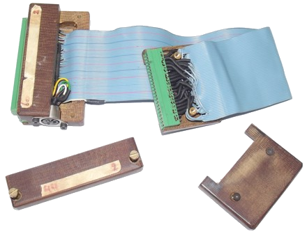 |
The ribbon cable has a connector at each end, one to mate with the console side port, and the other with the same pinout as the expansion card connectors in the PEB. The connectors are mounted in paxolin blocks which have been cut, milled and drilled - very tidy work. The 5-pin DIN plug is for connecting an external power supply to power the disk controller card. The whole arrangement is entirely passive apart from five 47Ω pullup resistors (to +5V) on pins 12, 16, 45, 46, 48 at the expansion card end which perform the function of those normally found on the flex cable interface card in the PEB (the flex cable interface card also has pullup resistors on pin 13 and 15, but these pins are not connected through the ribbon cable). Further detailed photos of the ribbon cable can be seen here, here and here. The connections between the two connectors on the ribbon cable are detailed in the table further down this page. The sliding door has to be removed from the console side port to enable the connector at the console end of the cable to fit, and the connector wiggled a little so it slips past the metal earthing fingers each side of the console connector. The disk controller card has been modified to disconnect the +5V, +12V and -5V voltage regulators and strap the power supplies straight through onto the card, allowing the use of an external regulated power supply. A few of the TTL ICs are socketed and presumably have been replaced at some point in the past. A picture of a standard card is available here. |
Getting the disk system to work proved to be an interesting experience ...
First I had to disassemble the disk controller end of the cable to determine the wiring to the DIN plug used for power to the disk controller. As the disk controller card has been modified to accept regulated supplies directly, it can be conveniently powered from an old PC ATX power supply that can also power the floppy drives themselves, so I wired up a DIN plug to connect with the power plug at the end of the cable.
So with the cable connected to the console, power connected to the cable, but the disk controller card not connected, the console boots fine. Connect the disk controller card however and the console hangs immediately power is applied. So out with the multimeter and check for shorts to ground on each of the disk controller card connector pins. This reveals that the READY signal has a resistance of only 20Ω to ground. It is driven by a 74LS125, so remove the old one, fit a socket and pop a new one in. The console now boots fine with the disk controller connected.
Powering on the console doesn't give the usual brief flash from the disk controller card LED as the DSR power up routine is executed. So out with the MiniMem cartridge and use EasyBug to 'switch on' the card by writing a 1 to CRU address >1100. The disk controller card LED now lights so it looks like the CRU circuit is working. Now looking at memory locations >4000 onward should read the DSR from the disk controller card ROMs, but only 00s are returned. So use the logic probe to start checking the inputs to the PAL U18; nothing obviously wrong here from a quick check. Checking the PAL outputs, the logic probe doesn't give a signal on the line to the 74LS245 data buffer U3 /OE pin. Checking this with a multimeter shows a voltage of ~1.8V, in the indeterminate range between a logic 0 and a logic 1. The 'LS245 is already socketed (and heatsinked via a small block of aluminium stuck to the inside of the clam shell) so has been replaced before – this particular type of IC can be prone to failure. Remove it and the output from the PAL starts registering on the logic probe. Checking the 'LS245 itself, the /OE pin has a resistance of approximately 80Ω to ground, so replace that, and the output from the PAL still registers on the logic probe. Still no joy though reading the contents of the disk controller card DSR ROMs. Looking at the inputs to the PAL a bit closer, there is no activity on the /MEMEN input. Tracing this signal back, the /MEMEN input to the 74LS244 buffer U5 is floating – the signal is not getting down the cable from the console. Take the cable connectors apart again to trace the signal through the cable, and /MEMEN is routed down the outer-most wire on one edge of the ribbon cable. This had been trapped years before when the connectors were assembled – the cable wasn't quite aligned in the shallow cutout between the two halves of the block, and the insulation was completely flattened. I had noticed this before, but hadn't thought that the wire within could also be broken, which it actually was. I managed a neat repair with a short length of wire from a spare piece of ribbon cable. Everything assembled again, power on the console and the disk controller card LED now gives the usual brief flash, and using EasyBug I can now read the contents of the DSR ROMs.
Next stage is to look at the drives. First, on one of the drives the sector mark sensor (photodiode) has broken off its base and this is fixed with a little bit of glue.
So, connect power to the first drive and switch on. Smoke! Resistor R22 on the floppy PCB is glowing gently red! Oh dear. Let's try the second drive. Smoke! Resistor R22 on the second drive is also gently glowing. Checking both boards, one side of R22 is shorted to ground, and the culprit – electrolytic capacitor C3 has shorted on *both* boards. Snipping one end of C3 temporarily allows testing to continue; I'll replace them and the charred resistors later. Experimenting with the drives, which are double-sided, yields the following results: on one drive only the bottom head is working (will only format single-sided), and on the second drive, both heads appear to be working (can format double-sided). The PCB on one of the drives is also faulty – any disk operation gives disk error 16 "no disk or no drive". Looking at the circuit diagram (a comprehensive instruction manual for the Siemens FDD200-5 drive is included in the manual for the Siemens PU 670C Programming Unit), the outputs from the floppy drive to the controller are all open-collector and gated by the drive select signal so that multiple drives can be connected on the same ribbon cable. Checking a few of the outputs with the logic probe while trying to access the drives – nothing. Tracing the drive select signal through the circuit identifies a 74LS14 inverter with a stuck output so remove it, fit a socket and pop a new one in and both drives now working.
Running the Disk Manager comprehensive test on each drive for a while reveals no further problems.
The connections between the two connectors on the ribbon cable are detailed in the table below.
Remember that you will need to provide a power source for the expansion card, either supplies at the same voltages as the PEB if leaving the voltage regulators in the expansion card in place, or regulated 5/12V supplies if bypassing the regulators in the card. Check and check again that the power supplies are correct before connecting!
| Expansion Card Connector |
Signal | Console Side Port Connector |
|
| 60 | +12V regulator supply | ||
| 59 | +12V regulator supply | ||
| 58 | -12V regulator supply | ||
| 57 | -12V regulator supply | ||
| 56 | /MEMEN ----------------------------------- | 32 | |
| 55 | CRUIN ------------------------------------ | 33 | |
| 54 | /WE --------------------------------------- | 26 | |
| 53 | --- N/C (GND) | ||
| 52 | DBIN -------------------------------------- | 9 | |
| 51 | /CRUCLK ---------------------------------- | 22 | |
| 50 | /CLKOUT ---------------------------------- | 24 | |
| 49 | --- N/C (GND) | ||
| 48 | Pullup to +5V (AMC) | ||
| 47 | GND -------------------------------------- | 23 | |
| 46 | Pullup to +5V (AMA) | ||
| 45 | Pullup to +5V (AMB) | ||
| 44 | A1 ---------------------------------------- | 30 | |
| 43 | A0 ---------------------------------------- | 31 | |
| 42 | A3 ---------------------------------------- | 10 | |
| 41 | A2 ---------------------------------------- | 20 | |
| 40 | A5 ---------------------------------------- | 5 | |
| 39 | A4 ---------------------------------------- | 7 | |
| 38 | A7 ---------------------------------------- | 17 | |
| 37 | A6 ---------------------------------------- | 29 | |
| 36 | A9 ---------------------------------------- | 18 | |
| 35 | A8 ---------------------------------------- | 14 | |
| 34 | A11 --------------------------------------- | 8 | |
| 33 | A10 --------------------------------------- | 6 | |
| 32 | A13 --------------------------------------- | 15 | |
| 31 | A12 --------------------------------------- | 11 | |
| 30 | A15 /CRUOUT ---------------------------- | 19 | |
| 29 | A14 --------------------------------------- | 16 | |
| 28 | D0 ---------------------------------------- | 37 | |
| 27 | --- N/C (GND) | ||
| 26 | D2 ---------------------------------------- | 39 | |
| 25 | D1 ---------------------------------------- | 40 | |
| 24 | D4 ---------------------------------------- | 35 | |
| 23 | D3 ---------------------------------------- | 42 | |
| 22 | D6 ---------------------------------------- | 36 | |
| 21 | D5 ---------------------------------------- | 38 | |
| 20 | --- N/C (GND) | ||
| 19 | D7 ---------------------------------------- | 34 | |
| 18 | --- N/C (/LOAD) | ||
| 17 | --- N/C (/INTA) | ||
| 16 | Pullup to +5V (/SENILB) | ||
| 15 | --- N/C (/SENILA) | ||
| 14 | --- N/C (IAQHA) | ||
| 13 | --- N/C (/HOLD)) | ||
| 12 | Pullup to +5V (PCBEN) | ||
| 11 | --- N/C (/RDBENA) | ||
| 10 | --- N/C (AUDIOIN) | ||
| 9 | --- N/C (/LCP) | ||
| 8 | --- N/C (SCLK) | ||
| 7 | --- N/C (GND) | ||
| 6 | /RESET ----------------------------------- | 3 | |
| 5 | --- N/C (GND) | ||
| 4 | READY ------------------------------------ | 12 | |
| 3 | GND -------------------------------------- | 21 | |
| 2 | +5V regulator supply | ||
| 1 | +5V regulator supply | ||
A useful check to perform on a faulty disk controller card (either a controller card in the PEB or a sidecar model) is to see if the card Device Service Routine (DSR) can be read. The DSR is stored in a ROM or EPROM on the card and contains a table of the device names supported by the card and the software to control these devices. When a command that involves a device is executed, such as OLD DSK1.PROGRAM, the computer switches on each controller card fitted to the system in turn and searches for the device name ("DSK1") in the device name table on that card. If it finds a match, the computer uses the software in that card's DSR to process the command. If the computer cannot find a matching device name on any card, an OLD command should return error code 50 (when using TI BASIC) or error code 00 (when using TI Extended BASIC). If you get this error code trying to load a program from disk, this suggests a problem reading the DSR on the disk controller card.
Reading the DSR on a disk controller card can be easily checked using either of two cartridges: a MiniMem cartridge, or a TI Extended BASIC cartridge. The technique using the MiniMem cartridge will work on just a bare console with disk controller attached. The technique using the Extended BASIC cartridge also requires 32K memory expansion to be present.
To check reading the disk controller card DSR using a MiniMem cartridge, proceed as follows:
Note that the technique using the MiniMem cartridge should also work if a fault with the disk controller card causes the console to lock up if powered on when the PEB is also powered on. Simply power off the PEB, power on the console, then power on the PEB, then proceed as above.
The same technique can also be used with other PEB cards by substituting the card's CRU address after the C command.
To check reading the disk controller card DSR using a TI Extended BASIC cartridge, type in the following Extended BASIC program:
10 CALL INIT
20 CALL LOAD(-16384,2,12,17,0,29,0,4,91)
30 CALL LOAD(-31804,192,0)
40 DIM B(8)
50 ADDR=16384
60 FOR A=ADDR TO ADDR+72 STEP 8
70 CALL PEEK(A,B(1),B(2),B(3),B(4),B(5),B(6),B(7),B(8))
80 FOR L=1 TO 8
90 PRINT STR$(B(L))&" ";
100 NEXT L
110 PRINT
120 FOR L=1 TO 8
130 IF B(L)<32 THEN PRINT "."; ELSE PRINT CHR$(B(L));
140 NEXT L
150 PRINT
160 NEXT A
[For those interested in how the program works, line 20 loads a small machine code program at address >C000 which sets register R12 to >1100, sets CRU bit 0 to "1" to 'switch on' the disk controller card, then returns. Line 30 sets the interrupt hook at address >83C4 to >C000 which runs the program. (Credit to Mizapf on AtariAge for this neat little bit of code which is more efficient than the code I first wrote.) Line 50 sets the variable ADDR to address >4000, which is the address of the start of the DSR. Line 60 sets up a loop to process the first 72 bytes of the DSR, in groups of 8 bytes. Line 70 reads each block of 8 bytes from the DSR. The loop starting at line 80 prints the value of each byte in decimal. The loop starting at line 120 prints the ASCII character represented by each byte (or a "." for non-printable byte values less than 32); printing the ASCII makes it easier to see device names in the DSR).]
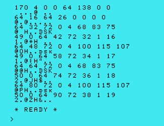
Running the program should give results similar to the screenshot below, showing lines of 8 bytes of data read from the DSR in decimal then those same bytes as ASCII on the line below. For any brand of disk controller card, the first four numbers should be 170 (>AA), then a low number or zero, then two zeroes. The data after that varies by type of disk controller card (the screen below shows the DSR used by the Classic99 emulator). For a standard TI disk controller card, you can see the data (in hexadecimal) here. You can easily look for the device names supported by the DSR ("DSK") in the ASCII part of the listing (to do this for the TI disk controller card, you'll probably have to change the number in line 50 from 16384 to 16416 as the device names are further into the DSR).
If the DSR data looks correct and you can see the device names, then the disk problem most likely lies with the floppy drives, the cable, or the floppy controller or associated circuitry on the card (but the DSR circuitry on the card appears to be OK).
If the DSR data looks corrupt (and you're absolutely sure you typed in the Extended BASIC program correctly!) then you're probably looking at diagnosing and repairing a hardware fault on the card.
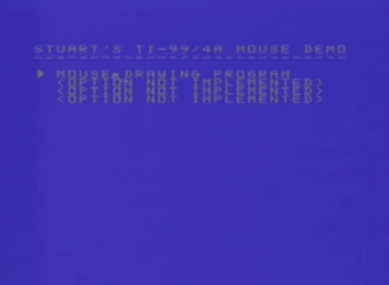
| A standard, old PC serial mouse can be connected directly to the serial port on a TI-99/4A nanoPEB interface. The listing below is for a mouse-driven menu and a simple sketch program. The listing also provides an example of how to initialise and control the RS-232 port, and how to plot individual pixels with the TMS 9918A VDP in graphics 2 mode. There is a video of the program in use here. The program can be downloaded on a TiDisk format image here. Copy the disk image to a spare volume on your nanoPEB. To run the program, boot with the Editor/Assembler cartridge, select E/A option 3, type the filename DSKn.MOUSE_O then the program name START. I've tried two serial mice which both work - labelled on the bottom as a Microsoft "Serial Mouse 2.1A", and a Microsoft "Serial - PS/2 Compatible Mouse". |
  |
******************************************************************************
*Experiment using a PC serial mouse connected to the serial port on a NanoPEB.
*The program first displays a mouse-driven menu, which is configured in
*Graphics 1 mode and uses a sprite defined as the mouse pointer. Selecting the
*first menu option runs a simple sketch application which is configured in
*Graphics 2 mode, giving a resolution of 256 x 192. Instructions for using the
*sketch application are displayed on screen.
*
*Mouse protocol details reference: www.kryslix.com/nsfaq/Q.12.html
*TMS9918A VDP datasheet: http://ftp.whtech.com/datasheets%20and%20manuals/
* Datasheets%20-%20TI/TMS9918.pdf
******************************************************************************
AORG >A000
DEF START
REF VSBW VDP single byte write.
REF VMBW VDP multiple byte write.
REF GPLLNK GPL routine link.
*************
*Definitions.
*************
*Graphics 1 mode storage in VRAM.
PNTBA1 EQU >0000 Pattern name table base address.
PGTBA1 EQU >0800 Pattern generator table base address.
CTBA1 EQU >0380 Colour table base address.
SATBA1 EQU >1B00 Sprite attribute table base address.
SGTBA1 EQU >3800 Sprite generator table base address.
*Graphics 2 (bitmap) mode storage in VRAM.
PNTBA2 EQU >1800 Pattern name table base address.
PGTBA2 EQU >0000 Pattern generator table base address.
CTBA2 EQU >2000 Colour table base address.
SATBA2 EQU SATBA1 Sprite attribute table base address.
SGTBA2 EQU SGTBA1 Sprite generator table base address.
*Memory mapped I/O definitions.
VDPREG EQU >8C02 VDP VRAM address and register access address.
VRAMW EQU >8C00 VDP VRAM data write address.
VRAMR EQU >8800 VDP VRAM data read address.
*CRU base address definitions.
BACARD EQU >1300 NanoPEB serial interface base address.
BA9902 EQU >1340 NanoPEB serial port 1 base address.
*******
*Start.
*******
START LWPI MYWS Load workspace.
******************************
*Initialise mouse RS-232 port.
******************************
*Switch on serial interface.
LI R12,BACARD
SBO 0
*Set port 1 to 1200 Baud, 7 data bits, no parity, 1 stop bit.
LI R12,BA9902 CRU base address of 9902 in NanoPEB.
SBO 31 Reset 9902. This sets /RTS inactive high, so the
* RTS output line to -ve voltage.
LI R1,>8200 Control register: 1 stop bit, no parity, 7 data
* bits (binary 10000010).
LDCR R1,8 Load control register.
SBZ 13 Disable loading of interval register.
LI R1,>01A0 1200 Baud.
LDCR R1,12 Load transmit and receive data rate registers.
SBO 16 Set /RTS active low, so the RTS output line to +ve
* voltage to power the mouse.
**************************************************************************
*Set up Graphics 1 mode.
*(Will already be in Graphics 1 mode after starting the program from E/A,
* but need routine to set up this mode when returning to the menu from the
* mouse drawing program which uses Graphics 2 mode.)
**************************************************************************
*Load VDP registers.
GRAPH1 BL @LOADER
BYTE >00,>80 Register 0 - graphics 1 mode, external video off.
BYTE >E0,>81 Register 1 - 16K, display on, interrupts on,
* graphics 1, size mag = 0.
BYTE >00,>82 Register 2 - PNTBA1 = >0000. Pattern name table.
BYTE >0E,>83 Register 3 - CTBA1 = >0380. Colour table.
BYTE >01,>84 Register 4 - PGTBA1 = >0800. Pattern generator
* table.
BYTE >36,>85 Register 5 - SATBA1 = >1B00. Sprite attribute
* table.
BYTE >07,>86 Register 6 - SGTBA1 = >3800. Sprite generator
* table.
BYTE >F5,>87 Register 7 - Backdrop=background colour.
DATA 0
*Clear the sprite generator table (SGT) and sprite attribute table (SAT).
BL @CLRSPR
*Load character set (character codes >20 - >5F) (from E/A manual page 251).
CLR R1 Clear GPL STATUS byte.
MOVB R1,@>837C
LI R1,8*>20+PGTBA1 Address in VDP RAM to load character set.
MOV R1,@>834A
BLWP @GPLLNK
DATA >0018
*Load colour table.
LI R8,CTBA1+>4000 Reference CT. Add >4000 for VDP write operations.
BL @SENDAD Send VDP address.
LI R11,256/8 Set count.
LI R1,>F500 Colour - white on light blue.
CTGRH1 MOVB R1,*R7 Write to colour table.
DEC R11 Done all entries?
JNE CTGRH1 No, loop around.
*Redefine characters:
* 96 for the menu selection pointer.
* 97 for inverse video 'H'.
* 98 for inverse video 'E'.
* 99 for inverse video 'R'.
LI R0,96*8+>0800 Offset of >0800 as PGT starts at >0800.
LI R1,MSPDAT
LI R2,8*4
BLWP @VMBW
*********************************
*Display menu in Graphics 1 mode.
*********************************
*Clear screen.
MNMENU BL @CLRSCN
*Display menu text.
CLR R0
LI R1,TXT1
MOV @TXT1L,R2
BLWP @VMBW
LI R0,32*3
LI R1,TXT2
MOV @TXT2L,R2
BLWP @VMBW
***********************************************************
*Define mouse pointer sprite and place at middle of screen.
***********************************************************
BL @DEFMSE
*Initialise mouse position to the middle of the screen.
*Mouse position range is twice the screen resolution (twice 192 x 256) to get
*an adequate movement of the mouse. The mouse position will be divided by two
*to map it to screen coordinates. (Can't divide mouse movement by two
*otherwise very slow movement will result in no movement.)
LI R9,256/2*2 Mouse X position in LSB.
MOV R9,@MSXPOS
LI R9,192/2*2 Mouse Y position in LSB.
MOV R9,@MSYPOS
**********************************************************************
*Get mouse position and display indicator against menu option if mouse
*Y position is on the same line.
**********************************************************************
GMPOS BL @UPDTMS Update mouse position.
MOV @MSYPOS,R9 Get mouse Y position.
SRL R9,4 Divide by 2, then by 8 to convert from pixels
* to lines.
LI R4,3 Menu start line number.
LI R5,6 Menu end line number.
LI R0,3*32+2 Menu pointer display position for top line.
MEN01 LI R1,' '*256 Default to no menu pointer for this line.
C R9,R4 Mouse on this line?
JNE MEN02 No, jump.
LI R1,96*256 Yes, select menu selection pointer character.
MEN02 BLWP @VSBW Display or remove menu pointer for this line.
C R4,R5 Done last line of menu?
JEQ CHKBTN Yes, jump.
AI R0,32 No, do next line of menu.
INC R4
JMP MEN01
************************************************************
*Mouse left button clicked? If yes then jump to menu option.
************************************************************
CHKBTN MOV @MSBTTN,R1
COC @H6000,R1 Check for left mouse button pressed.
JNE GMPOS Left button not pressed, jump.
CI R9,3 Button pressed when on first line of menu?
JEQ MENU01 Yes, jump to menu.
CI R9,4 Button pressed when on second line of menu?
JEQ MENU02 Yes, jump to menu.
CI R9,5 -- Ditto --
JEQ MENU02
CI R9,6
JEQ MENU02
JMP GMPOS Button not pressed when mouse on menu line.
********************
*Menu option 1 text.
********************
*Clear screen.
MENU01 BL @CLRSCN
*Display instruction text for paint program.
CLR R0
LI R1,TXT3
MOV @TXT3L,R2
BLWP @VMBW
LI R0,32*3
LI R1,TXT4
MOV @TXT4L,R2
BLWP @VMBW
LI R0,32*23+5
LI R1,TXT6
MOV @TXT6L,R2
BLWP @VMBW
*Loop until mouse clicked on 'HERE' on bottom line.
BL @WAITHR
*Jump to drawing program.
JMP RSTART
*************************
*Menu options 2 - 4 text.
*************************
*Clear screen.
MENU02 BL @CLRSCN
*Display 'menu option not implemented' text.
CLR R0
LI R1,TXT5
MOV @TXT5L,R2
BLWP @VMBW
LI R0,32*23+5
LI R1,TXT6
MOV @TXT6L,R2
BLWP @VMBW
*Loop until mouse clicked on 'HERE' on bottom line.
BL @WAITHR
*Return to main menu.
JMP MNMENU
******************************************************************************
* MOUSE DRAWING PROGRAM *
******************************************************************************
************************
*Set up Graphics 2 mode.
************************
*Load VDP registers.
RSTART BL @LOADER
BYTE >02,>80 Register 0 - graphics 2 mode, external video off.
BYTE >80,>81 Register 1 - 16K, no display, no interrupt,
* graphics 2, size mag = 0.
BYTE >06,>82 Register 2 - PNTBA2 = >1800. Pattern name table.
BYTE >FF,>83 Register 3 - CTBA2 = >2000. Colour table.
BYTE >03,>84 Register 4 - PGTBA2 = >0000. Pattern generator
* table.
BYTE >36,>85 Register 5 - SATBA2 = >1B00. Sprite attribute
* table.
BYTE >07,>86 Register 6 - SGTBA2 = >3800. Sprite generator
* table.
BYTE >00,>87 Register 7 - Backdrop=background colour.
DATA 0
*Clear the sprite generator table (SGT) and sprite attribute table (SAT).
BL @CLRSPR
*Set up pattern name table.
LI R8,PNTBA2+>4000 Reference PNT. Add >4000 for VDP write
* operations.
BL @SENDAD Send VDP address.
SETO R11 Reset count.
INIPNT INC R11 Next pattern.
SWPB R11 Position LS byte.
MOVB R11,*R7 Write it.
SWPB R11 Restore R11.
CI R11,3*256 Done all entries?
JL INIPNT No, loop around.
*Set up pattern generator table.
LI R8,PGTBA2+>4000 Reference PGT. Add >4000 for VDP write
* operations.
BL @SENDAD Send VDP address.
LI R11,3*256*8 Set count.
KILPGT MOVB @B00,*R7 Reset entry.
DEC R11 Done all entries?
JNE KILPGT No, loop around.
*Set up colour table.
LI R8,CTBA2+>4000 Reference CT. Add >4000 for VDP write operations.
BL @SENDAD Send VDP address.
CLR R1 Clear R1 because we'll be shifting left.
MOVB @MPTSAT+3,R1 Get initial mouse pointer sprite colour.
SLA R1,4 Shift to left nibble to align with foreground
* colour in CT.
MOVB R1,@MSCOL Store initial mouse pointer colour.
LI R11,3*256*8 Set count.
INICT MOVB R1,*R7 Set colour to initial mouse pointer sprite colour.
DEC R11 Done all entries?
JNE INICT No, loop around.
*Re-enable display.
BL @LOADER
BYTE >C0,>81
DATA 0
***********************************************************
*Define mouse pointer sprite and place at middle of screen.
***********************************************************
BL @DEFMSE
LI R9,256/2*2 Mouse X position in LSB.
MOV R9,@MSXPOS
LI R9,192/2*2 Mouse Y position in LSB.
MOV R9,@MSYPOS
***********************
*Update mouse position.
***********************
WAIT1 BL @UPDTMS
*************************************************************************
*Check for left and right buttons pressed together. If pressed, return to
*main menu.
**************************************************************************
MOV @MSBTTN,R1
COC @H7000,R1 Check for left and right button indication in 1st
* byte received.
JNE CLRSCR Left and right button not both pressed, jump.
B @GRAPH1 Return to main menu.
***********************************************************************
*Check for right button press. If pressed, change mouse pointer colour.
***********************************************************************
CLRSCR COC @H5000,R1 Check for right button indication in 1st byte
* received.
JNE UPDCL1 Right button not pressed, jump.
AB @H10,@MSCOL Right button pressed. Move onto next colour.
JNE UPDCOL Need to wrap colour index back round? No, jump.
MOVB @H20,@MSCOL Reset colour to 2, skipping transparent and black
* colours.
UPDCOL LI R8,SATBA2+>4000+3 Reference colour byte in SAT. Add >4000 for
* VDP write operations.
BL @SENDAD Send VDP address.
MOVB @MSCOL,R2 Get stored colour.
SRL R2,4 Shift to 2nd nibble to align with colour nibble in
* SAT.
MOVB R2,*R7 Write new colour to mouse pointer sprite.
***********************************************************************
*Check for left button press. If pressed, draw pixel at mouse position.
***********************************************************************
UPDCL1 COC @H6000,R1 Check for left button indication in 1st byte
* received.
JNE DRWEX Left button not pressed, jump.
*Convert mouse X position to column number and remainder.
MOV @MSXPOS,R2 Get X position (which is at twice screen
* resolution).
MOV R2,R3 Copy it.
SRL R2,4 Divide by 2 to convert to screen resolution, then
* divide by 8 to get column number.
SRL R3,1 Divide by 2 to convert to screen resolution.
ANDI R3,>0007 Get 3 LS bits which are the remainder
* (the pixel 0 to 7 within the 8-pixel column).
*Convert mouse Y position to row number and remainder.
MOV @MSYPOS,R8 Get Y position (which is at twice screen
* resolution).
MOV R8,R9 Copy it.
SRL R8,4 Divide by 2 to convert to screen resolution, then
* divide by 8 to get row number.
SRL R9,1 Divide by 2 to convert to screen resolution.
ANDI R9,>0007 Get 3 LS bits which are the remainder
* (the pixel 0 to 7 within the 8-pixel row).
*Multiply row number by 32, then add column number to get cell number.
SLA R8,5 Multiply row number by 32.
A R2,R8 Add column number.
*Multiply cell number by 8 to get index into entry in the PGT for this cell
*(8 bytes in PGT per cell, 1 per pixel row).
SLA R8,3 Multiply cell number by 8.
*Get current VRAM data from cell number, add new pixel, and write back to
*VRAM.
A R9,R8 Add Y remainder to get correct byte in PGT for the
* pixel row.
BL @SENDAD Send cell address to VDP.
CLR R10 Clear pixel mask register. The pixel mask gives
* the bit to set in the PGT byte for the pixel
* 0 to 7 within the 8-pixel column.
AI R3,MASKTB Add address of pixel mask table base to
* X remainder.
MOVB *R3,R10 Fetch pixel mask.
MOVB @VRAMR,R3 Get current VRAM data.
SOCB R10,R3 Set pixel bit.
ORI R8,>4000 Set VDP write bit in address.
BL @SENDAD Send address to VDP.
MOVB R3,*R7 Write updated VRAM data.
*Set the colour table entry to the current mouse pointer sprite colour.
AI R8,CTBA2-PGTBA2 Get address of PCT entry.
BL @SENDAD Send address to VDP.
MOVB @MSCOL,*R7 Update colour entry.
********************************
*Loop round and do it all again.
********************************
DRWEX B @WAIT1
*************
*************
*Subroutines.
*************
*************
**************************************************
*Load the VDP registers from an inline data table.
**************************************************
LOADER MOVB *R11+,@VDPREG Write register data.
C *R11,*R11 Dummy delay for VDP.
MOVB *R11+,@VDPREG Write register number.
MOV *R11,*R11 End of data table?
JNE LOADER No, loop.
INCT R11 Yes, skip data table terminator.
B *R11 Return.
***********************************
*Send the address in R8 to the VDP.
***********************************
SENDAD SWPB R8 Position LSB.
MOVB R8,@VDPREG Send LSB.
SWPB R8 Position MSB.
MOVB R8,@VDPREG Send MSB.
B *R11 Return.
*************************************************************************
*Clear the sprite generator table (SGT) and sprite attribute table (SAT).
*************************************************************************
CLRSPR MOV R11,@SAVR11 Save return address.
LI R7,VRAMW
LI R8,SGTBA1+>4000 Reference SGT. Add >4000 for VDP write
* operations.
BL @SENDAD Send VDP address.
LI R8,256*8 Do 256 8-bit patterns.
KILSGT MOVB @B00,*R7 Null out the pattern.
DEC R8 Count it.
JNE KILSGT Loop till all done.
LI R8,SATBA1+>4000 Reference SAT. Add >4000 for VDP write
* operations.
BL @SENDAD Send VDP address.
LI R8,32*8 Kill off all 32 sprite planes.
LI R6,>D000 Fill it full of sprite terminators.
KILSAT MOVB R6,*R7 Clear SAT.
DEC R8 Count it.
JNE KILSAT Loop till all done.
MOV @SAVR11,R11 Restore return address.
B *R11 Return.
**************
*Clear screen.
**************
CLRSCN CLR R0 Start writing at start of screen image table.
LI R1,' '*256 Space character.
LI R2,32*24-1 Number of characters to do - but do 1 outside
* loop.
BLWP @VSBW Write one byte.
CLR1 MOVB R1,@VRAMW Write successive bytes without doing a BLWP -
* quicker.
DEC R2
JNE CLR1
B *R11
***********************************************************
*Define mouse pointer sprite and place at middle of screen.
***********************************************************
*Write character pattern to the sprite generator table.
DEFMSE MOV R11,@SAVR11 Save return address.
LI R8,SGTBA1+>4000 Reference SGT. Add >4000 for VDP write
* operations.
BL @SENDAD Send VDP address.
LI R8,8 Do one 8-bit pattern.
LI R6,MPTSPG Pointer to character pattern.
MPTRSG MOVB *R6+,*R7 Write the pattern.
DEC R8 Count it.
JNE MPTRSG Loop till all done.
*Define sprite in the sprite attribute table.
LI R8,SATBA1+>4000 Reference SAT. Add >4000 for VDP write
* operations.
BL @SENDAD Send VDP address.
LI R8,4 4 bytes to write.
LI R6,MPTSAT Pointer to SAT for mouse pointer.
MPTRSA MOVB *R6+,*R7 Write the SAT.
DEC R8 Count it.
JNE MPTRSA Loop till all done.
MOV @SAVR11,R11 Restore return address.
B *R11 Return.
********************************************************
*Wait for a packet of data from the mouse.
*Determine the mouse movement and update mouse position.
*Move mouse pointer sprite.
********************************************************
**
*Wait for and store a packet of 3 bytes. The first byte of each packet should
*be a value greater than or equal to >40. Check for this to keep reception in
*sync.
**
UPDTMS LI R12,BA9902 CRU base address of 9902 in NanoPEB.
CLR R1
CLR R2
CLR R3
WAIT3 TB 21 Receive buffer register full?
JNE WAIT3 No, loop until a character is received.
STCR R1,8 Read character into MSB of R1.
SBZ 18 Reset receive buffer register.
CI R1,>4000 Bit set to indicate first byte in packet?
JL WAIT3 No, get another byte.
WAIT4 TB 21 Receive buffer register full?
JNE WAIT4 No, loop until a character is received.
STCR R2,8 Read character into MSB of R2.
SBZ 18 Reset receive buffer register.
WAIT5 TB 21 Receive buffer register full?
JNE WAIT5 No, loop until a character is received.
STCR R3,8 Read character into MSB of R3.
SBZ 18 Reset receive buffer register.
MOV R1,@MSBTTN Save mouse buttons pressed data.
**
*Determine the mouse movement and update mouse position.
**
*Determine the X movement.
MOV R1,R5 Copy byte 1.
SLA R5,6 Move MS bits of X movement to top of byte.
A R5,R2 Add to rest of X movement in 2nd byte.
SWPB R2 Move result into LSB.
*Determine the Y movement.
MOV R1,R5 Copy byte 1.
ANDI R5,>0C00 Isolate bits 2 and 3.
SLA R5,4 Shift to move MS bits of Y movement to top of
* byte.
A R5,R3 Add to rest of Y movement in 3rd byte.
SWPB R3 Move result into LSB.
*Update mouse X position.
MOV @MSXPOS,R9 Get stored mouse X position.
CI R2,128 Is X movement left (-ve) or right (+ve)?
JLE UPDTX1 Jump if to the right.
AI R2,>FF00 Movement is to the left. Change to two's
* complement word.
A R2,R9 Subtract (add two's complement) movement from
* mouse X position.
JGT UPDTX2 If position now > 0, it's valid.
JEQ UPDTX2 If position now 0, it's valid.
CLR R9 Result is < 0, so reset position to 0.
JMP UPDTX2
UPDTX1 A R2,R9 Add movement to X position.
CI R9,2*255 If X position > 2*255 then set to 2*255.
JLE UPDTX2
LI R9,2*255
UPDTX2 MOV R9,@MSXPOS Store new mouse X position.
*Update mouse Y position.
MOV @MSYPOS,R9 Get stored mouse Y position.
CI R3,128 Is Y movement up (-ve) or down (+ve)?
JLE UPDTY1 Jump if down.
AI R3,>FF00 Movement is up. Change to two's complement word.
A R3,R9 Subtract (add two's complement) movement from
* mouse Y position.
JGT UPDTY2 If position now > 0, it's valid.
JEQ UPDTY2 If position now 0, it's valid.
CLR R9 Result is < 0, so reset position to 0.
JMP UPDTY2
UPDTY1 A R3,R9 Add movement to Y position.
CI R9,2*191 If Y position > 2*191 then set to 2*191.
JLE UPDTY2
LI R9,2*191
UPDTY2 MOV R9,@MSYPOS Store new mouse Y position.
**
*Move mouse pointer sprite.
**
*First byte in SAT is vertical position, second byte is horizontal position.
MOVMS MOV R11,@SAVR11 Save return address.
LI R8,SATBA1+>4000 Reference SAT. Add >4000 for VDP write
* operations.
BL @SENDAD Send VDP address.
MOV @MSYPOS,R2 Get stored mouse Y position (which is at twice
* screen resolution).
DECT R2 Top row of the screen has value -1, so adjust.
SLA R2,7 Move to MSB and divide by 2 to convert to screen
* resolution.
MOVB R2,*R7 Write the Y mouse position.
MOV @MSXPOS,R2 Get stored mouse X position (which is at twice
* screen resolution).
SLA R2,7 Move to MSB and divide by 2 to convert to screen
* resolution.
MOVB R2,*R7 Write the X mouse position.
MOV @SAVR11,R11 Restore return address.
B *R11 Return.
***************************************************
*Loop until mouse clicked on 'HERE' on bottom line.
***************************************************
WAITHR MOV R11,@SAVR12 Save return address.
WAHR01 BL @UPDTMS Update mouse position.
MOV @MSBTTN,R1
COC @H6000,R1 Check for left mouse button pressed.
JNE WAHR01 Left button not pressed, jump.
MOV @MSYPOS,R9 Get mouse Y position.
SRL R9,4 Divide by 2, then by 8 to convert from pixels
* to lines.
CI R9,23 Mouse on bottom line of screen?
JNE WAHR01 No, jump.
MOV @MSXPOS,R9 Get mouse X position.
SRL R9,4 Divide by 2, then by 8 to convert from pixels
* to characters.
CI R9,11 Mouse over the correct characters?
JL WAHR01 No, jump.
CI R9,14
JH WAHR01 No, jump.
MOV @SAVR12,R11 Yes, restore return address.
B *R11 Return.
**************************
*Workspace, text and data.
**************************
MYWS BSS 32 Workspace.
TXT1 TEXT ' STUART''S TI-99/4A MOUSE DEMO '
TEXT ' ----------------------------'
TXT1L DATA $-TXT1
TXT2 TEXT ' MOUSE DRAWING PROGRAM '
TEXT ' (OPTION NOT IMPLEMENTED) '
TEXT ' (OPTION NOT IMPLEMENTED) '
TEXT ' (OPTION NOT IMPLEMENTED) '
TXT2L DATA $-TXT2
TXT3 TEXT ' SKETCH PROGRAM INSTRUCTIONS '
TEXT ' ---------------------------'
TXT3L DATA $-TXT3
TXT4 TEXT 'USE THE MOUSE TO MOVE THE '
TEXT 'POINTER AROUND THE SCREEN. HOLD '
TEXT 'DOWN THE LEFT MOUSE BUTTON TO '
TEXT 'DRAW AS YOU GO. CLICK THE RIGHT '
TEXT 'MOUSE BUTTON TO CHANGE THE PEN '
TEXT 'COLOUR. '
TEXT ' '
TEXT 'CLICK BOTH MOUSE BUTTONS '
TEXT 'TOGETHER TO RETURN TO THE MENU.'
TXT4L DATA $-TXT4
TXT5 TEXT '*** THIS MENU OPTION IS NOT *** '
TEXT '*** IMPLEMENTED ***'
TXT5L DATA $-TXT5
TXT6 TEXT 'CLICK '
BYTE 97,98,99,98 'HERE' using video inverse characters.
TEXT ' TO CONTINUE'
TXT6L DATA $-TXT6
EVEN
SAVR11 DATA 0 Saved return address.
SAVR12 DATA 0 Second saved return address.
MSXPOS DATA 0 Mouse X position in LSB.
MSYPOS DATA 0 Mouse Y position in LSB.
MSBTTN DATA 0 Mouse buttons pressed.
MSCOL BYTE 0 Mouse pointer colour.
B00 BYTE 0
B16 BYTE 16
H10 BYTE >10
H20 BYTE >20
H5000 DATA >5000
H6000 DATA >6000
H7000 DATA >7000
*Mouse pointer sprite data.
MPTSPG BYTE >F8,>F0,>F0,>D0,>88,>04,>02,>01 Arrow pattern.
MPTSAT BYTE 192/2-1,256/2,>00,>0F Initial position middle of screen, colour
* white.
*Menu selection pointer character data.
MSPDAT BYTE >10,>18,>1C,>1E,>1E,>1C,>18,>10
*'HER' in inverse video characters data.
BYTE >00,>BB,>BB,>BB,>83,>BB,>BB,>BB
BYTE >00,>83,>BF,>BF,>87,>BF,>BF,>83
BYTE >00,>87,>BB,>BB,>87,>AF,>B7,>BB
*Pixel bit mask table.
*Pixel------- 0 1 2 3 4 5 6 7
MASKTB DATA >8040,>2010,>0804,>0201
END
This is a web browser for the TI-99/4A (and now also ported to the Geneve), where the TI-99 is connected to the Internet using one of the following methods:
The browser will not work with any 'modern' web pages - there are just too many HTML tags and other stuff for the TI to handle, and there's no way you could display much of it anyway with the TI's low resolution screen. Instead, the browser works with a bespoke set of tags which are matched to the display capabilities of the TI-99.
The latest version of the browser is v9.4, which runs on a TIPI only. This version has been ported to the Geneve running under MDOS and connected to a TIPI. Most of the information below is common to both the TI-99 and Geneve versions (they both support the same tags and render screens in the same way), with some information specific to the Geneve version and a download link included here.
The program is on a TiDisk format image which can be downloaded here. Extract the TiDisk file from the zip file, then upload it to the root directory of the TIPI using the TIPI web interface. The TIPI will automatically extract the files into a directory named "BROWSER".
To run the program, boot with the Editor/Assembler cartridge, select E/A option 3 and type the filename TIPI.BROWSER.INTERNET (or DSK.BROWSER.INTERNET). The program will automatically start after loading.
The program is available as a FinalGROM99 image here. The program needs some of the files on the TiDisk image above in order to run, so you still need to download that TiDisk format image and upload it to the TIPI.
If using a mouse (connected to the Raspberry Pi) to control the browser, try using the oldest USB mouse you have available and move the mouse slowly. A newer mouse with a high resolution can make the browser pointer hard to control.
To be clear, all versions that support a serial port do not include the latest browser functionality. Use of the latest TIPI version is recommended.
The Lantronix UDS-10 will need this configuration for Channel 1:
NOTE: The configuration has been changed from that used for browser v9.0 and earlier. Note the different Baudrate and I/F Mode settings. These settings are required for browser v9.1 and later.
I usually configure the Lantronix over Telnet - the Lantronix User Guide contains details for doing this. I have problems configuring the Lantronix through the built-in web app - the Connect Mode Settings:Response field usually gets reset to the default setting each time I open the web app, rather than showing the current setting.
The Lantronix is wired to the serial port on a NanoPEB as follows:
NanoPEB Lantronix
9-way D-type Male 25-way D-type Female
Pin Pin
2 (RX) ------<<------ (RX out) 3
3 (TX) ------>>------ (TX in) 2
5 (GND) -------------- (GND) 7
7 (RTS) -->>--+
8 (CTS) --<<--+ (pins 7 and 8 connected together)
The Lantronix is wired to the 1st serial port on a TI PEB RS-232 card as follows:
RS-232 Card Lantronix
25-way D-type Female 25-way D-type Female
Pin Pin
2 (RD-1) ------<<----- (RX out) 3
3 (TX-1) ------>>----- (TX in) 2
5 (CTS-1) ----->>----- (RTS in) 4
7 (GND) -------------- (GND) 7
20 (DTR-1) ----<<----- (CTS out) 5
Various download options are available, depending on how you intend to run the program. Download links are in the table below, with a description of the various options below that.
| Disk Image | 32K EPROM Image, Inverted Bank Switching |
32K EPROM Image, Non-Inverted Bank Switching |
512K EPROM Image, Non-Inverted Bank Switching |
| Internet Browser v9_2.zip | Internet Browser 32K Inverted v9_2.zip | Internet Browser 32K Non‑Inverted v9_2.zip | Internet Browser 512K Non‑Inverted v9_2.zip |
The program is on a TiDisk format image and named "INTERNET". To run the program, boot with the Editor/Assembler cartridge, select E/A option 3 and type the filename DSKn.INTERNET. After loading, the program name required depends on the type of RS-232 port you're using:
This is a binary image which can be burned into a 32K 27(C)256 EPROM for use on a 64K 'Guidry' bank-switched cartridge board fitted with a 74LS379 (inverted outputs) latch. The option to select from the master selection list depends on the type of RS-232 port you're using:
This is a binary image which will work with a FlashROM99 cartridge.
The option to select from the master selection list depends on the type of RS-232 port you're using, as detailed for the 32K inverted EPROM image above.
This is a binary image which can be used as follows:
The option to select from the master selection list depends on the type of RS-232 port you're using, as detailed for the 32K inverted EPROM image above.
With the cartridge versions of the program, you still need a disk file DSK.BROWSER.FAVS to use the favourites list, described below.
When the program starts, it displays an instruction page and prompts for the web page to load at the top of the screen. The "www." prefix is provided already (backspace over this for a host name without a "www." prefix or to enter an IP address). The URLs of some sample web sites are given further down this page. The web page address is limited to 80 characters. Use lower-case for the web page address - ALPHA LOCK up!
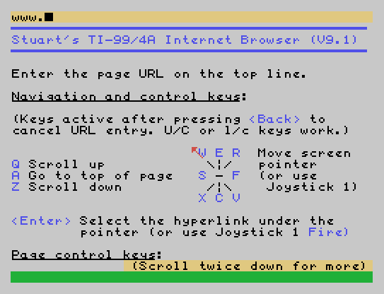
After entering a web page address, the program shows status messages at the bottom of the screen as it resolves the server IP address (for the serial port version) then downloads the web page. With the serial port version, the Lantronix sometimes experiences a problem connecting to a web server - if the program says it is retrying the connection, it normally succeeds after 30 seconds or so.
The navigation and control keys supported are as follows (these can be entered as either upper or lower case):
The keys auto-repeat to make it easier to move the pointer between hyperlinks.
The pointer can also be moved horizontally, vertically and diagonally using a joystick or (for the TIPI version) USB mouse connected to the Raspberry Pi. The joystick Fire button or left mouse button select any hyperlink, input field or submit button that the pointer is over.
From browser version v9.3 onwards, clicking on the first 3 character positions of the URL address bar prompts for entry of a new page URL (the same action as pressing the N key). Clicking on any other character position of the URL address bar displays the current URL for editing (the same action as pressing <Fctn>-E).
With the serial port version, pressing any key when the program is retrying a connection will abort the connection and prompt for a new URL. (Note that it may take a couple of seconds for the program to respond after pressing the key.)
When entering or editing text in an input field, the following control keys are active:
The program supports a list of favourites, which is displayed by pressing the I key. This loads and renders the contents of the file TIPI.BROWSER.FAVS (or DSK.BROWSER.FAVS). This is written/edited by the user using (for example) the E/A Editor, and saved in 'Variable 80' format. The file contains text and tags for hyperlinks to the user's favourite pages - it is in effect a web page stored on the disk. As well as hyperlinks, the page can contain any graphics or character definitions desired by the user. Long lines of text/tags can be split across several lines in the file. A sample file is included on the disk.
|
www.stuartconner.me.uk/tibrowser/browser_help_tipi_92.htm (for browser v9.2) www.stuartconner.me.uk/tibrowser/browser_help_tipi_93.htm (for browser v9.3) www.stuartconner.me.uk/tibrowser/browser_help_tipi_94.htm (for browser v9.4) |
A page showing the same instructions displayed when the program initially loads. |
| www.stuartconner.me.uk/tibrowser/z.htm www.stuartconner.me.uk/tibrowser/z_ti_test_2.htm www.stuartconner.me.uk/tibrowser/z_ti_test_3.htm |
A set of linked pages demonstrating the capabilities of
the program. A screenshot of the first page is shown
here. The second page gives a
short history of the TI-99/4A. The third page shows the pinout of the
TMS 9900 processor. |
| www.stuartconner.me.uk/tibrowser/tichat.php www.stuartconner.me.uk/tibrowser/tichat.php?m=your_text |
There is a simple chat application. Use the first URL on the left to view the current messages. To add a message to the page, add to the end of the same URL "?m=your_text" (without the quotes, and with underscores instead of spaces). Remember that the max length of the entire URL is 80 characters. |
| www.stuartconner.me.uk/tibrowser/getclientipaddress.php | Displays the external IP address of your home network. |
| www.stuartconner.me.uk/tibrowser/getdatetime.php | Displays the local date and time on the (US) host server. |
|
www.stuartconner.me.uk/tibrowser/getweather.php?l=city,country code Example: www.stuartconner.me.uk/tibrowser/getweather.php?l=southampton,gb *** Page not working at the moment - I need to check it *** |
Displays the current weather at the specified city, which is
identified by the city name and 2-character country code (the "Alpha-2
code" on
this
page). If the city name contains a space, replace it with an
underscore, for example: ?l=new_york,us. The location is not
case-sensitive. |
| www.stuartconner.me.uk/tibrowser/getwebipaddress.php?w=domain Example: www.stuartconner.me.uk/tibrowser/getwebipaddress.php?w=news.bbc.co.uk |
Displays the numeric IP address of the domain specified
by [domain]. |
| www.stuartconner.me.uk/tibrowser/valley.htm | Graphics demo page. |
| www.stuartconner.me.uk/tibrowser/elite.htm | Graphics demo pages. The program automatically cycles
through a sequence of pages. |
| www.myti99.com | This is by far the most sophisticated site yet supporting the TI web browser, and is developed and maintained by Corey Anderson. To make use of most of the site you first need to register a user name and password by accessing the site www.myti99.com from your PC (or direct from the browser if using v9.3 onwards), then you can access the same site from your TI for applications such as an impressive 2-player chess game. |
The screenshots below show a few sample web pages.
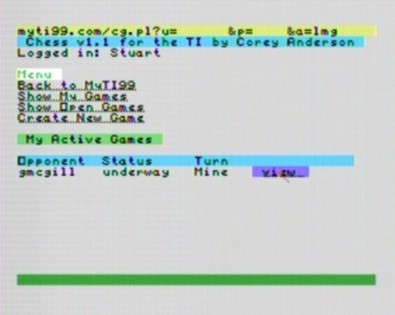
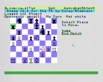
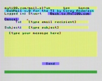
As well as web servers specified by host name, v9.2 onwards of the browser also supports web servers specified by IP address. So the following example web page URL formats are supported:
With the first two URL formats above where a host name is given, if using a serial port version of the browser, the browser accesses a script on a web page on the server 64.037.052.172 (which hosts my site www.stuartconner.me.uk) to resolve the specified host name to its IP address.
The URL in a hyperlink on a page can specify either a host name or an IP address.
The tags supported are listed in the table below. Note that the tags are CASE sensitive. Example usage of the more complex tags is given in later sections.
| Tag | Description | ||||||||||||||
| <99ml> | Indicates start of page. All text before this tag is ignored. | ||||||||||||||
| </99ml> | Indicates end of page. All text after this tag is ignored. | ||||||||||||||
| <p> | Indicates start of a paragraph. All text outside <p></p> tags is treated as a comment and ignored. | ||||||||||||||
| </p> | Indicates end of a paragraph. The following text is rendered starting on the next line on the screen. | ||||||||||||||
| <br> | Line break. The following text is rendered starting on the next line on the screen. | ||||||||||||||
| <a:(URL)> | Specifies a hyperlink for the text following the tag. | ||||||||||||||
| </a> | Indicates end of hyperlink text. | ||||||||||||||
| <arect:AA:BB:CC:DD:(URL)> | Defines a rectangular link area defined in pixels. AA, BB, CC and DD are upper-case hex values. If the <Return> key or <Fire> button is pressed, then if the screen pointer X position (in pixels, relative to the top left of the screen) is between the values AA and BB (inclusive) and the screen pointer Y position is between the values CC and DD (inclusive), then the link is invoked, and the specified URL is called with “?x=(pointer X position in hex)&y=(pointer Y position in hex)” appended to the URL (or "&x=..." if the link URL already contains a "?"). (Note that the screen pointer moves in steps of 2 pixels.) | ||||||||||||||
| <u> | Underlines the text following the tag. | ||||||||||||||
| </u> | Indicates end of underline text. | ||||||||||||||
| <clr:(foreground colour code)(background colour code)> | Render the characters following the tag in the specified colours. The colour code
definitions are given below. Characters are 6 pixels wide so are not aligned with the 8-pixel blocks used by the VDP for colour control. Controlling text colour on a paragraph by paragraph basis will work. If trying to change text colour mid-paragraph, the results will depend on whether the start/end characters are exactly aligned with the edge of an 8-pixel block. |
||||||||||||||
| </clr> | Revert back to normal colours (black on grey). | ||||||||||||||
| <cdef:(character code in hex):(hex character def)> | Redefine the specified character. Characters in the range >00 to >FF are supported. The default character definitions are automatically reloaded when browsing to a new page. Characters have to be defined BEFORE they are used. The same characters can be redefined several times on the same page - define each with the pattern needed before using them. The default character definitions are: - Character >00 is a special character used internally and should not be redefined. - Character >01 is a special character used internally and should not be redefined on a page that uses input fields. - Character >0A is defined as a Line Feed character. - Character >0D is defined as a Carriage Return character. - Characters >0E - >18 are defined with table drawing characters, as follows: - Character >0E - ┏ top left corner - Character >0F - ━ horizontal line - Character >10 - ┳ top join - Character >11 - ┓ top right corner - Character >12 - ┃ vertical line - Character >13 - ┣ left vertical join - Character >14 - ╋ centre join - Character >15 - ┫ right vertical join - Character >16 - ┗ bottom left corner - Character >17 - ┻ bottom join - Character >18 - ┛ bottom right corner - Characters >20 - >7E are defined as the normal ASCII character set. - Character >7F is defined as a solid block. - (All other characters are defined as blank) |
||||||||||||||
| <chr_lt> | Displays the '<' character (this 'alias' is needed in order to be able to display tags on the screen as text). | ||||||||||||||
| <chr:(character code in hex)> | Displays the specified character. | ||||||||||||||
| <8pchr:(character code in hex):(character position in hex, 2 bytes)> | Render all 8 pixel columns of the specified character at the specified position. The position is based on the screen divided into 8*8 tiles, so positions are numbered from 0 (top left) to 767 (bottom right). This tag is provided for plotting graphics where the character rendering is exactly aligned with the VDP colour table. | ||||||||||||||
| <8pclr:(character colour in hex, 8 bytes)> | Defines the colours used for characters
rendered using the <8pchr> tag. Each byte of the colour code specifies
the colour of one row of the 8x8 character. The first nibble of each
byte specifies the foreground colour, and the second byte specifies the
background colour. The colour code definitions are given below. The default foreground and background colours are both transparent. Note that the colour information is loaded to VDP RAM as the tags are processed, so colour changes to the currently displayed page might be seen as a new page is rendered. |
||||||||||||||
| <ptrclr:(sprite colour code)> | Changes the colour of the sprite pointer. The sprite colour code is two hex characters, the first of which must be 0 and the second the required sprite colour according to the colour code definitions given below. | ||||||||||||||
| <noscroll> | Disables the keyboard scroll keys on a web page. This is intended for web pages designed for display as a single page and using the <8pchr> and/or <arect> tags which don't work as intended if the page is scrolled down. | ||||||||||||||
| <noclearscreen> | Disables clearing the screen when rendering a new web page. This enables one web page to update the screen rendered by the previous web page (so for example one web page could draw half a complex graphic on the screen and a second web page draw the other half). | ||||||||||||||
| <loadpage:(URL)> | Displays the screen rendered so far then loads the specified web page. | ||||||||||||||
| <updatescreen> | Displays the screen rendered by the tags processed so far, then continues processing tags on the page. | ||||||||||||||
| <startrenderline:(line number in hex, 2
bytes)> (browser v9.4 onwards) |
Specifies which line of the web page to display at the top of the screen when the page is initially displayed. As an example, if the tag is <startrenderline:0012>, the 18th line of the web page is initially displayed at the top of the screen. An example use of this tag is for a message page where the most recent message is initially displayed, and the user can then scroll up the page to see older messages. | ||||||||||||||
| <input:(foreground colour code)(background colour code):(tag ID)> | Defines the start of a text input field.
When the user clicks on an input field, they can type into the field,
terminating input by pressing <Enter>. When the user then clicks on a
submit field 'button', the tag ID and entered value of each input field
on the page are appended as parameters to the end of the URL specified
by the <submit> tag. The tag ID must be an alphanumeric string and
can be up to 96 characters long. The foreground and background colour control enables the field to easily be made a different colour to the surrounding text to make the field itself and the field length prominent. |
||||||||||||||
| </input> | Defines the end of an input field. The field length is determined by the number of characters between the <input> and </input> tags. These characters may be spaces or some sort of text prompt. With the <input> tag, these characters are not a default field value - the reported field value is an empty string unless the user types a value into the field. | ||||||||||||||
| <input-dv:(foreground colour code)(background
colour code):(num characters):(tag ID)> (browser v9.3 onwards) |
Same as the <input> tag but the (num characters) parameter (one hex byte) specifies the number of characters between the <input-dv> and </input-dv> tags to use as a default field value. This is the field value reported unless the user types a different value into the field. | ||||||||||||||
| </input-dv> (browser v9.3 onwards) |
Defines the end of an input-dv field. | ||||||||||||||
| <pwd:(foreground colour code)(background
colour code):(tag ID)> (browser v9.3 onwards) |
Same as the <input> tag but any non-space characters typed into the field are displayed as asterisks, to obscure entered information such as a password. | ||||||||||||||
| </pwd> (browser v9.3 onwards) |
Defines the end of a password field. | ||||||||||||||
| <submit:(foreground colour code)(background colour code):(URL)> | Defines the start of a submit field
'button'. The text between the <submit> and </submit> tags is displayed
as the button caption. When the user clicks on the button, the tag ID
and value of each input, input-dv and password field on the page are appended as
a parameter to the end of the URL specified by the <submit> field.
The total length of the URL is limited to 100 characters, so only a
small number of fairly short fields can be used. The URL is
added to the URL history. The foreground and background colour control enables the button to easily be made a different colour to the surrounding text to make it prominent. |
||||||||||||||
| </submit> | Defines the end of a submit field. | ||||||||||||||
| <submit-nh:(foreground colour code)(background colour code):(URL)> | Same as the <submit> tag but the URL is not added to the URL history and the 100-character URL length limit does not apply. This allows far longer input fields to be used. | ||||||||||||||
| <cookie:(cookie value)> (browser v9.3 onwards) |
Stores a cookie value to be associated with the host name from which the page was downloaded. Cookie details are stored in a COOKIES file on the TIPI disk, and so are persistent across browser sessions. The cookie value is included in the HTTP request header for all future page requests to the same host. | ||||||||||||||
| <timeout:(period):(URL)> | Loads a new page (or refreshes the current
page) when no user input (keyboard or joystick movement) is made for the
timeout period. The timeout period, in seconds, is specified as one hex
byte. For example, a value '14' gives a timeout period of 20 seconds.
The URL specifies the page to go to, and can be the same URL as the
current page
to refresh the page, or a different URL to go to a different page. The timeout period should be fairly accurate for a conventional TI-99/4A with the 32K RAM on the 8-bit bus and normal wait states. For a TI with the 32K RAM on the 16-bus, the actual timeout period will be approx 10-20% less than the specified value. |
||||||||||||||
| <favs> (browser v9.3 onwards) |
Defines the start of a hyperlink that displays the user's favourites file. | ||||||||||||||
| </favs> (browser v9.3 onwards) |
Defines the end of a favourites hyperlink. | ||||||||||||||
| <tone:(duration):(volume):(frequency index)> | Plays a tone on the speaker. The tone duration,
in units of 1/10th of a second, is specified as one hex byte. Volume is
in the range 00 (minimum volume (silence)) to 0F (maximum volume). The
frequency is specified as the index value in the frequency table below.
For example, the tag <tone:1E:0F:18> plays 'middle A' (440 Hz) at full
volume for 3 seconds.
|
The colour codes used by the <clr>, <8pclr>, <ptrclr>, <input>, <input-dv>, <pwd> and <submit> tags are as follows:
| 0 - Transparent | 8 - Medium Red |
| 1 - Black | 9 - Light Red |
| 2 - Medium Green | A - Dark Yellow |
| 3 - Light Green | B - Light Yellow |
| 4 - Dark Blue | C - Dark Green |
| 5 - Light Blue | D - Magenta |
| 6 - Dark Red | E - Grey |
| 7 - Cyan | F - White (Note: A-F must be upper-case) |
The diagram below shows some example text character patterns. Each character is 6 pixels wide - the right-most 2 columns in the 8-pixel character block are not used. To define these patterns for characters >80 and >81, use the following <cdef> tags:
<cdef:80:0038443008443800>
<cdef:81:0038101010103800>
These characters can then be used in text displayed using the <p></p> tags. The <chr> tag can be used to specify a particular character code to display. The <clr> tag enables the text colour to be specified - each character has a single foreground colour and a single background colour. See the web page listing below for examples.
Although 'graphics' could be displayed by defining and displaying text characters (as shown by the TI logo in the example web page listing and screenshot below), using the <8pchr> and <8pclr> tags provides more flexibility and colour control.
Using the <8pchr> tag, all 8 pixel columns of a character definition are displayed. To define the patterns below for characters >A0 and >A1, use the following <cdef> tags:
<cdef:A0:8040201008040201>
<cdef:A1:8142241818244281>
When using the <8pchr> tag, each character is displayed at a specified position. The position is based on the screen divided into 8*8 tiles, so positions are numbered from 0 (top left) to 767 (bottom right) - 24 rows of 32 tiles. To display the two characters above as the first two characters on row 3 of the screen:
<8pchr:A0:0040>
<8pchr:A1:0041>
Note that the character code must be exactly two upper-case hex digits and the character position must be exactly four upper-case hex digits.
To set the colour for a character, use the <8pclr> tag, where the colour is specified by 8 bytes. Each byte of the colour code specifies the colour of one row of the 8x8 character. The first nibble of each byte specifies the foreground colour, and the second byte specifies the background colour. The colour specified by an <8pclr> tag is stored for use by all following <8pchr> tags until changed by another <8pclr> tag. The default foreground and background colours for displaying characters using the <8pchr> tag are both transparent. The following example displays the two characters above, the first character as dark red on light yellow, and the second character as a rainbow effect on a black background.
<8pclr:6B6B6B6B6B6B6B6B><8pchr:A0:0040>
<8pclr:21416181A1C1E1F1><8pchr:A1:0041>

Characters displayed using <8pchr> tags can be mixed with text displayed using the <p></p> tags. If displayed in the same position on the screen, whichever tags occur later in the web page source overwrite those that occur earlier in the page source.
As characters displayed using the <8pchr> tag are displayed at fixed positions on the screen, they cannot be scrolled. Consider including the <noscroll> tag on a page where <8pchr> tags are used to disable the keyboard scroll keys.
If wanting to display a very complex graphic, the 13,024 byte (from v8.2 onwards) web page size limitation might be an issue. This can be worked around by drawing part of the screen on one page, using the <loadpage> tag at the end of that page to automatically load a second page, including the <noclearscreen> tag at the top of the second page and continuing to draw the graphic. Obviously though there will be a delay while the second page loads. The same technique can be used for simple animation by drawing a main graphic then automatically loading a further sequence of pages to draw updates over that graphic. An example <loadpage> tag is:
<loadpage:www.stuartconnerdownloads.me.uk/tibrowser/elite_2.htm>
The <a></a> tags enable hyperlinks over text displayed with the <p></p> tags. To place hyperlinks over graphics, use the <arect> tag, which has the format <arect:AA:BB:CC:DD:(URL)>. AA, BB, CC and DD are upper-case hex values which define a rectangular area of pixels relative to the top left of the screen. If the <Return> key or <Fire> button is pressed, then if the screen pointer X position (in pixels, relative to the top left of the screen) is between the values AA and BB (inclusive) and the screen pointer Y position is between the values CC and DD (inclusive), then the link is invoked, and the specified URL is called with "?x=(pointer X position in hex)&y=(pointer Y position in hex)" appended to the URL (or "&x=..." if the link URL already contains a "?"). (Note that the screen pointer moves in steps of 2 pixels.)
Looking at the part of the page below, to place a hyperlink over the black cross, AA has the value 8, BB has the value 16, CC is 16 and DD is 24. With these values in hex, this gives the following <arect> tag:
<arect:08:10:10:18:www.stuartconnerdownloads...>
Many <arect> tags can be used on a page. If any of the hyperlink areas overlap, clicking on an overlapping area selects the first of the overlapping hyperlinks defined in the web page source.
As the pointer position is appended to the hyperlink URL when the hyperlink is selected, this information can be further processed if required by a script on the linked page. For example, if hyperlinks are required over a chess board graphic, rather than defining one hyperlink per chess board square, define one hyperlink over the complete board then process the pointer information returned in the hyperlink URL to determine which square the pointer was over.
The page timeout feature loads a new page (or refreshes the current page) when no user input (keyboard or joystick movement) is made for the timeout period. The page listing for the screenshot below includes an example page timeout tag.
The <timeout> tag specifies a timeout period (of between 0 and 255 seconds, expressed as one hex byte) and a URL. The program calls the specified URL when no user input is made for the timeout period. The URL can be the same URL as the current page to refresh the page, or a different URL to go to a different page. The timeout period should be fairly accurate for a conventional TI-99/4A with the 32K RAM on the 8-bit bus and normal wait states. For a TI with the 32K RAM on the 16-bus, the actual timeout period will be approx 10-20% less than the specified value.
Note that with a long web page where the user has to scroll down to see the entire page, the <timeout> tag only takes effect if the tag is in the code for the section of the page currently displayed, or in a 'higher' area of the page. If the user has not yet scrolled down far enough to view the section of the page that contains the <timeout> tag, the tag has no effect. This feature can be used to design a page that automatically refreshes if the user is viewing the end of the page, but stops refreshing if the user then scrolls up to view earlier content.
Text input fields and a submit 'button' enable interactive web sites to request information from the user. The screenshot below and the corresponding page listing below that illustrate the use of these features.
Browser versions up to and including v9.2 support just one type of input field, defined by a pair of <input></input> tags. The <input> tag specifies the field colour and a unique (on that page) tag ID. When the user clicks on an input field, they can type into the field, terminating input by pressing <Enter>. The field length is determined by the number of characters between the <input> and </input> tags. These characters may be spaces or some sort of text prompt. Note that these characters are not a default field value - the reported field value is considered to be blank until the user types a value into the field.
Browser version v9.3 onwards supports two additional types of input field:
A submit 'button' is defined by a pair of <submit></submit> tags or <submit-nh></submit> tags. The <submit(-nh)> tag specifies the field colour and a URL. The text between the <submit(-nh)> and </submit> tags is displayed as the button caption.
With the <submit> tag, when the user clicks on a submit field 'button', the tag ID and value of each input, input-dv and password field on the page are appended as parameters to the end of the URL specified by the <submit> tag. Looking at the example below, if the user types the text "Stuart" into the first field and "Conner" into the second field then clicks the Submit button, the program calls the URL "www.somesite.com?fn=Stuart&ln=Conner". Note that when appending the input field values to the URL, any "<space>", "#", "&", ";", "=" or "?" characters are encoded into their "%xx" equivalents. The total length of the URL is limited to 100 characters, so only a small number of fairly short input fields can be used. The URL is added to the URL history.
To work around the 100-character URL length limit when a larger number of fields or longer fields are needed, use the <submit-nh> tag. This supports a total URL length of many hundreds of characters (the exact number depends on what else is on the page), but the URL is not added to the URL history.
Two further points when using the input field and submit tags:
<99ml>
<p><br>Enter·first·name:·<input:1A:fn>(first·name)·······
</input></p>
<p><br>Enter·last·name:··<input:1A:ln>(last·name)········
</input></p>
<p><br><br>·········<submit:1C:www.somesite.com>Submit</submit></p>
<timeout:3C:www.someothersite.com>
</99ml>
If redisplaying the page and the two field values are already known, input-dv fields can be used instead to specify default field values so that the user does not have to enter them again:
<p><br>Enter·first·name:·<input-dv:1A:06:fn>Stuart·············
</input-dv></p>
<p><br>Enter·last·name:··<input-dv:1A:06:ln>Conner·············
</input-dv></p>
To include a password field:
<p><br>Enter·password:·<pwd:1A:pw>········· </pwd></p>
When making HTTP GET calls, the browser identifies itself with a User-Agent parameter in the HTTP request header.
The User-Agent parameter enables a web page script to see it is talking to the TI browser and to format a page accordingly. Corey Anderson's www.myti99.com website uses the parameter to serve different versions of the site according to whether it is accessed from a PC or TI.
Browser v9.3 onwards supports a cookie mechanism implemented through the <cookie> tag. This tag specifies a cookie value to be associated with the host name from which the page was downloaded. Cookie details are stored in a COOKIES file on the TIPI disk, and so are persistent across browser sessions.
The cookie value is included in the HTTP request header for all future page requests to the same host. So if the page cookie_test.htm downloaded from www.stuartconner.me.uk contains the tag <cookie:some_cookie_value>, then all future HTTP page requests to www.stuartconner.me.uk will contain the parameter "Cookie: www.stuartconner.me.uk=some_cookie_value" in the HTTP request header.
Two further points when using cookies:
Browser versions up to and including v9.2 will only display pages where the HTTP response code is 200 (OK).
Browser version v9.3 onwards will display pages where the HTTP response code is 200 (OK) or 301 (new permanent URI). In addition, the browser will also display pages where the HTTP response code is 404 (page not found) or 500 (internal server error) as long as the error page includes content within <99ml></99ml> tags. This enables a server administrator to set up browser-compatible error pages for these response codes.
The following listing displays the example web page below which uses many of the supported tags. Space characters in the listing have been replaced with a small dot to aid legibility.
<99ml>
Character·definitions·for·TI·logo.
<cdef:01:7CC0C0C0C0C0C0C0>
<cdef:02:C0485454486020C0>
<cdef:03:0000000000003048>
<cdef:04:FC80C04060381C0C>
<cdef:05:C408080C000000B0>
<cdef:06:981818D858585840>
<cdef:07:E82828E884848488>
<cdef:08:F84C040400000000>
<cdef:09:24180084C4703C00>
<cdef:0A:3040800000808000>
Character·definition·for·bullet.
<cdef:0B:0000003030000000>
Colour·bar.
<p><br><clr:16>····<clr:13>····<clr:11>····<clr:1D>····<clr:14>····<clr:12>····<clr:18>····<clr:15>····<clr:19>····<clr:16>···</clr></p>
Blank·line·in·cyan.
<p><clr:17>·······································</clr></p>
TI·Logo·and·title·in·cyan.
<p><clr:17>··<chr:01><chr:02><chr:03>·<chr:0E><chr:0F><chr:0F><chr:0F><chr:0F><chr:0F><chr:0F><chr:0F><chr:0F><chr:0F><chr:0F><chr:0F><chr:0F><chr:0F><chr:0F><chr:0F><chr:0F><chr:0F><chr:0F><chr:0F><chr:0F><chr:0F><chr:0F><chr:0F><chr:0F><chr:0F><chr:0F><chr:0F><chr:0F><chr:0F><chr:0F><chr:0F><chr:11></clr></p>
<p><clr:17>·<chr:04><chr:05><chr:06><chr:07>·<chr:12>··TEXAS·INSTRUMENTS·COMPUTERS··<chr:12></clr></p>
<p><clr:17>··<chr:08><chr:09><chr:0A>·<chr:16><chr:0F><chr:0F><chr:0F><chr:0F><chr:0F><chr:0F><chr:0F><chr:0F><chr:0F><chr:0F><chr:0F><chr:0F><chr:0F><chr:0F><chr:0F><chr:0F><chr:0F><chr:0F><chr:0F><chr:0F><chr:0F><chr:0F><chr:0F><chr:0F><chr:0F><chr:0F><chr:0F><chr:0F><chr:0F><chr:0F><chr:0F><chr:18></clr></p>
Blank·line·in·cyan.
<p><clr:17>·······································</clr></p>
Colour·bar.
<p><clr:16>····<clr:13>····<clr:11>····<clr:1D>····<clr:14>····<clr:12>····<clr:18>····<clr:15>····<clr:19>····<clr:16>···</clr><br><br></p>
Menu.
<p><chr:0B>·Click·<a:www.stuartconner.me.uk/tibrowser/z_ti_test_2.htm>here</a>·for·a·short·history·of·the<br>··TI-99/4A.<br></p>
<p><chr:0B>·Click·<a:www.stuartconner.me.uk/tibrowser/z_ti_test_3.htm>here</a>·for·the·pinout·of·the<br>··TMS9900·processor.</p>
</99ml>
As an alternative to using the Lantronix UDS-10 serial-to-Ethernet adaptor, I have also written a small Python script which emulates the functionality of the UDS-10 as used by the browser. This script will work on a Raspberry Pi, Windows (XP or later) PC or Mac. So you can connect the serial port on your TI to a serial port on your Pi/PC/Mac, and run the script to process web connection requests from the TI. This section is aimed at Python and Pi novices to help you get this running.
The following instructions are for a Raspberry Pi 2 Model B (the Python script has also been tested on a Raspberry Pi 3 Model B). They assume a fresh install of the Raspbian operating system, you've got an Internet network connection configured, and that you've got a USB serial adaptor plugged in and connected to the serial port on your TI. The Python software and the Python serial port module should already be installed along with the Raspbian O/S.
The following instructions assume that you've got a COM serial port on your PC (and if it's a USB serial adaptor, you have the relevant drivers already loaded), and it is connected to the serial port on your TI.
The following instructions assume that you've got a USB serial adaptor connected to your Mac and you have the relevant drivers already loaded, and it is connected to the serial port on your TI. The Python software should already be installed (Python comes as standard on a Mac).
This section looks at an I2C - "I Squared C" or "Inter-Integrated Circuit" - interface for the TI-99. The ICs in your old VCR would have used an I2C interface to communicate with each other, and your digital STB likely uses one internally as well. Devices with an I2C interface are gaining popularity in the hobbyist market also because an I2C interface is one of the interfaces that comes as standard on the Raspberry Pi and Arduino. There are many types of I2C device available - LED drivers, LCD drivers, serial memory (RAM and EEPROM), clocks, analogue-to-digital converters, digital-to-analogue converters, and so on.
Electrically, the I2C interface is very simple - just two wires plus ground. One wire is for a clock (SCL) and the other is for serial data (SDA). When writing to a 'slave' device, the 'master' drives both the clock and the data lines. When reading from a slave device, the master controls the clock line and the slave drives the data line. Multiple devices can be connected to the clock and data lines. Each device has a unique address, and the master sends the address of the device to access before reading or writing data to it. The clock frequency is very flexible - most devices have an upper limit of about 100 kHz, and anything below that is OK.
So how can we use this on the TI? Well the joystick port has two lines that we can control individually, and we can feed the data line back in through a third pin to sense its state. All we need is a 74LS06 inverter and two pullup resistors hooked onto the joystick port. You'll need a +5V power supply as well. A circuit diagram is shown below. The components to the left of the joystick connector are existing circuits internal to the TI console and are shown for reference only. The components to the right of the joystick connector show the circuit you need to build.
A few notes about the circuit:
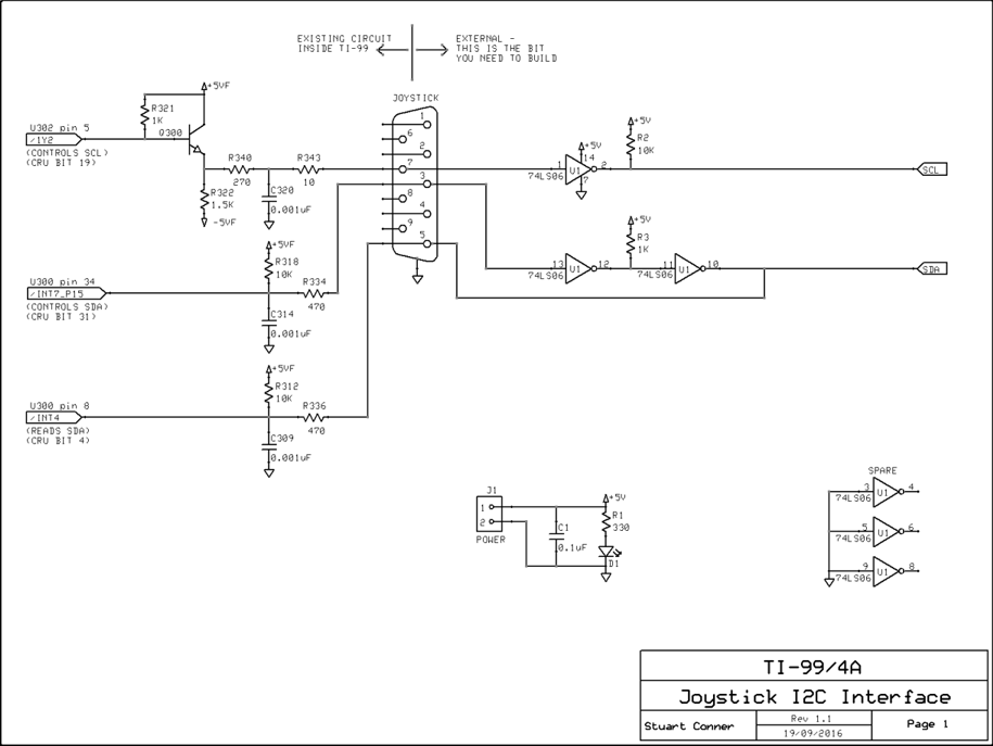
You won't be able to use the console keyboard scanning routine while using the I2C interface as that will send out some spurious signals over the interface (you actually need the interface powered down or disconnected for the keyboard to be read properly), but you could probably write a bespoke keyboard scanning routine that scans just certain keys on the keyboard matrix rows/columns that aren't connected to the joystick port. Oh - Alpha Lock needs to be up as well!
Software-wise, the code needs to be able to control pins on the joystick port directly over the CRU interface, so that means assembly code. It should be possible for an XB program (for example) to pass data to/from the assembly routines. Cortex BASIC should also work as that includes instructions to control the CRU interface. The routines fall into two groups:
For a simple proof of concept, the photo below shows the TI connected to a 20 character by 4 four line LCD display with an I2C interface - £7.00 on eBay. The LCD display itself has a parallel interface but comes with an I2C interface 'backboard' already soldered on that performs the serial I2C interface to parallel conversion. A pair of LEDs on the interface board helped with debugging. The code I've used to display a message on this is below.
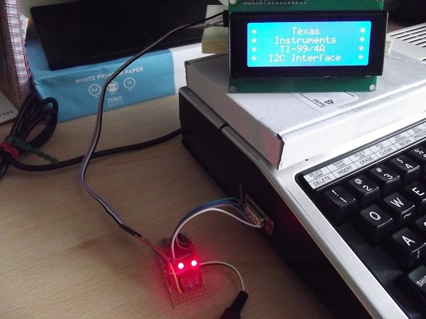
DEF START
SCL EQU 19 CRU BIT FOR SCL SIGNAL.
SDA EQU 31 CRU BIT FOR SDA SIGNAL.
START LWPI WS LOAD WORKSPACE.
LIMI 0 DISABLE ALL INTERRUPTS.
*CONFIGURE TMS9901.
CLR R12 9901 CRU BASE ADDRESS.
SBO 20 SET 9901 P4 HIGH TO SELECT DEMUX 1 IN U302.
SBZ 18 SET 9901 P2 (A) LOW ...
*TO CONTROL SCL:
*- SBO SCL TO SET SCL HIGH
*- SBZ SCL TO SET SCL LOW
*TO CONTROL SDA:
*- SBO SDA TO SET SDA HIGH
*- SBZ SDA TO SET SDA LOW
*SET INITIAL CONDITION, WITH SCL AND SDA BOTH HIGH.
SBO SCL
SBO SDA
BL @DELAY1
*INITIALISE POINTER TO ADDRESS/DATA TO SEND.
LI R4,I2CDAT
*SEND START SEQUENCE - SDA LOW, SCL REMAINS HIGH.
SBZ SDA
BL @DELAY1
*SEND I2C DEVICE ADDRESS.
MOVB *R4+,R9 GET ADDRESS INTO MSB OF R9.
BL @SNDBYT SEND ADDRESS.
*SEND COMMANDS AND DATA.
*HAVE TO SEND TO LCD DISPLAY AS TWO GROUPS OF 4 BITS,
*WITH CONTROL SIGNALS ALSO SET APPROPRIATELY.
*THIS SECTION OF CODE IS SPECIFIC TO THE TYPE OF I2C DEVICE
*BEING CONTROLLED.
GETBYT MOVB *R4+,R2 GET DATA INTO MSB OF R2.
CB R2,@BFF >FF TERMINATOR CHARACTER?
JEQ STOP YES, JUMP.
LI R7,>0900 RIGHT NIBBLE OF R7 CONTAIN DATA FOR LCD CONTROL PINS.
* SET TO STATE FOR SENDING AN ASCII CHARACTER
* (BACKLIGHT ON, RS HIGH, R/W LOW, E LOW).
CB R2,@B00 LCD DISPLAY CONTROL CHARACTER?
JNE GETBY2 NO, JUMP.
LI R7,>0800 YES. SET R7 TO STATE FOR SENDING AN LCD CNTRL CHAR
* (BACKLIGHT ON, RS LOW, R/W LOW, E LOW).
MOVB *R4+,R2 GET THE CHARACTER AFTER THE >00.
* DO LEFT NIBBLE.
GETBY2 MOVB R2,R5 MAKE COPY OF ORIGINAL DATA BYTE.
ANDI R5,>F000 SET ALL BITS OF RIGHT NIBBLE TO 0.
SOC R7,R5 SET STATE
OF BACKLIGHT, RS, R/W, E.
MOV R5,R8 COPY BYTE.
MOV R5,R9
BL @SNDBYT
ORI R5,>0400 SET E HIGH.
MOV R5,R9
BL @SNDBYT
MOV R8,R9 SET E LOW AGAIN.
BL @SNDBYT
* DO RIGHT NIBBLE.
MOVB R2,R5 COPY ORIGINAL DATA BYTE AGAIN.
SLA R5,4 SHIFT RIGHT NIBBLE TO LEFT NIBBLE.
ANDI R5,>F000 SET ALL BITS OF RIGHT NIBBLE TO 0.
SOC R7,R5 SET STATE OF BACKLIGHT, RS, R/W, E.
MOV R5,R8 COPY BYTE.
MOV R5,R9
BL @SNDBYT
ORI R5,>0400 SET E HIGH.
MOV R5,R9
BL @SNDBYT
MOV R8,R9 SET E LOW AGAIN.
BL @SNDBYT
JMP GETBYT DO NEXT BYTE.
*SEND STOP SEQUENCE - SDA TAKEN HIGH WHEN SCL ALREADY HIGH.
STOP SBZ SCL SET SCL LOW.
BL @DELAY2 WAIT 1/2 CLOCK PERIOD.
SBZ SDA SET SDA LOW AGAIN AFTER ACK BIT.
BL @DELAY2 WAIT 1/2 CLOCK PERIOD.
SBO SCL SET CLOCK HIGH.
BL @DELAY1 WAIT 1 CLOCK PERIOD.
SBO SDA SET SDA HIGH.
FINISH JMP FINISH LOOP FOREVER.
*
*SEND BYTE IN MSB OF R9.
*R9 IS DESTROYED.
*
SNDBYT MOV R11,@SAVR11 SAVE RETURN ADDRESS.
LI R3,8 LOAD BIT COUNTER.
SBITS SLA R9,1 SHIFT MSb OF BYTE INTO CARRY STATUS BIT.
JOC CARRY1
MOV @SBZ31,@SETSDA NO CARRY - WRITE OP-CODE TO ROUTINE BELOW.
JMP CARRY2
CARRY1 MOV @SBO31,@SETSDA CARRY - WRITE OP-CODE TO ROUTINE BELOW.
CARRY2 SBZ SCL SET SCL LOW.
BL @DELAY2 WAIT 1/2 CLOCK PERIOD.
SETSDA DATA >0000 SET SDA - OP-CODE WRITTEN ABOVE.
BL @DELAY2 WAIT 1/2 CLOCK PERIOD.
SBO SCL SET SCL HIGH.
BL @DELAY1 WAIT 1 CLOCK PERIOD.
DEC R3 INCREMENT BIT COUNTER.
JNE SBITS LOOP UNTIL ALL BITS DONE.
SBZ SCL SET CLOCK LOW.
BL @DELAY2 WAIT 1/2 CLOCK PERIOD.
SBO SDA SET SDA HIGH SO SLAVE CAN SEND ACK BIT.
BL @DELAY2 WAIT 1/2 CLOCK PERIOD.
SBO SCL SEND ANOTHER CLOCK PULSE FOR ACK BIT - IGNORE IT.
BL @DELAY1 WAIT 1 CLOCK PERIOD.
MOV @SAVR11,R11 RESTORE RETURN ADDRESS
B *R11 RETURN.
*
*DELAY LOOP - ONE PERIOD.
*
DLYPRD EQU >0002
DELAY1 LI R1,DLYPRD
DEL1 DEC R1
JNE DEL1
B *R11
*
*DELAY LOOP - HALF PERIOD.
*
DELAY2 LI R1,DLYPRD/2
JMP DEL1
*STORAGE.
WS BSS 32 PROGRAM WORKSPACE.
SAVR11 DATA >0000 SAVED RETURN ADDRESS FOR SUB-ROUTINES.
SBO31 DATA >1D1F OP-CODE FOR 'SBO 31'.
SBZ31 DATA >1E1F OP-CODE FOR 'SBZ 31'.
B00 BYTE >00
*NOTE ABOUT I2C ADDRESS:
*RASPBERRY PI REPORTS LCD DISPLAY AS ADDRESS >27.
*NEED TO SHIFT THAT LEFT ONE BIT AS THE LSb IS THE
R/W SIGNAL.
*SO NEED TO USE ADDRESS >4E TO WRITE, >4F TO READ.
*NOTE ABOUT I2C LCD DISPLAY DATA:
*PREFIX ALL DISPLAY INSTRUCTION (COMMAND) BYTES WITH >00.
*THIS IS USED TO SET THE DISPLAY RS PIN TO THE APPROPRIATE STATE.
*THE TEXT TO DISPLAY IS SEQUENTIAL ASCII CHARACTERS.
I2CDAT BYTE >4E I2C
INTERFACE IC ADDRESS. MUST IMMEDIATELY PRECEDE DATA.
BYTE >00,>33,>00,>32,>00,>06 COMMAND
BYTES TO CONFIGURE DISPLAY.
BYTE >00,>0C,>00,>28,>00,>01
BYTE >00,>80 COMMAND
BYTE TO ADDRESS LCD LINE 1.
TEXT '* Texas *' TEXT
FOR LINE 1.
BYTE >00,>C0 COMMAND
BYTE TO ADDRESS LCD LINE 2.
TEXT '* Instruments *' TEXT
FOR LINE 2.
BYTE >00,>94 COMMAND
BYTE TO ADDRESS LCD LINE 3.
TEXT '* TI-99/4A *' TEXT
FOR LINE 3.
BYTE >00,>D4 COMMAND
BYTE TO ADDRESS LCD LINE 4.
TEXT '* I2C Interface *' TEXT
FOR LINE 4.
BFF BYTE >FF TERMINATOR CHARACTER.
END
As stated above, the LCD display used in this proof of concept has a parallel interface but comes with an I2C interface 'backboard' already soldered on that performs the serial I2C interface to parallel conversion.
The I2C interface IC used on the 'backboard' is a PCF8574T (datasheet). This has 8 input/output pins, referred to as P0 - P7. When a byte is written to the IC, the first bit sent (the code above sends the MSb first) is output on pin P7, and the last bit sent (the LS bit of the byte) is output on pin P0.
The digital connections on the LCD display (datasheet 1 or datasheet 2) are:
Clearly the 8-bit output of the I2C interface IC is not able to simultaneously control the 11 digital connections to the LCD display, so the display is connected and configured into 4-bit interface mode where each byte of data is transferred as two reads/writes to data bits DB7 - DB4 (the higher 4 bits of data first, then the lower 4 bits of data), and data bits DB3 - DB0 on the display are unused and not connected. The two 4-bit data transfers have to be handled by the I2C master device through the interface IC. As only 4 bits of data are used for the display, this leaves 4 input/output pins on the I2C interface IC free for controlling the LCD display RS, R/W and E signals, also for switching the display backlight on and off (this latter function is implemented on the 'backboard' by controlling the power supply to the backlight - logic 1 switches the backlight on, and logic 0 switches the backlight off). The actual connections between the I2C interface IC and the LCD display are shown in the diagram below, which also shows the mapping of the bits in the byte written by the TI to the P0 - P7 pins on the I2C interface IC. As an example, to set RS high, the backlight on, and all other signals low, write the binary value 0000 1001 = >09. To set E high as well, write the binary value 0000 1101 = >0D.
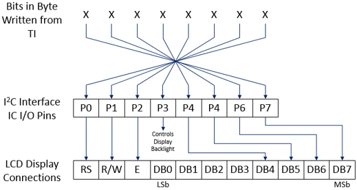
Writing an instruction (command) byte to the LCD display through the I2C interface IC requires the steps outlined below. These steps assume that the I2C interface IC address has already been sent, and that the code handles the setting of the start and stop sequences and the bit clock as detailed in the IC datasheet and the code comments above.
To write a data byte (a character or character pattern) to the LCD display requires the same steps but RS must be high instead of low. In the code above, instruction (command) bytes are prefixed with a >00 byte which is used to differentiate between instruction and data bytes so the state of the RS signal can be set accordingly.
The set of instruction (command) bytes initially sent to initialise the LCD display are as follows: (these are also detailed in the LCD display (datasheet 1 or datasheet 2)
TIPI is a storage, network and device expansion for the TI-99/4A that connects to an external Raspberry Pi device. It is available in sideport and PEB expansion card versions. Further details are available on the TIPI wiki.
The following code provides an example of using the TIPI network socket interface in assembly language to download a web page. The screenshot below shows the program output.
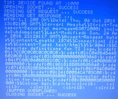
DEF START Program entry point.
REF VSBW VDP single byte write.
REF VMBW VDP multiple byte write.
REF VWTR VDP write to register.
GPLWS EQU >83E0 GPL workspace. For exchanging parameters with TIPI ROM routines.
GPLWSR0 EQU GPLWS Register 0 in GPL workspace.
GPLWSR1 EQU GPLWS+2 Register 1 in GPL workspace.
SENDMSG EQU >4012 Address holding address of send message routine in TIPI ROM.
RECVMSG EQU >4010 Ditto for address of receive message routine.
START LWPI MYWS Load program workspace.
****************************************************
*Switch to text mode (40 x 24).
****************************************************
*Set VDP register 1 to set text mode but with display disabled until we have set up the screen.
LI R0,>01B0 VDP register 1 - Text mode with display disabled.
BLWP @VWTR VDP write to register.
*Clear screen.
CLR R0 Start writing at start of screen image table.
LI R1,' '*256 <Space> character in MSB.
LI R2,960-1 960 characters to do - but do 1 outside loop.
BLWP @VSBW Write one byte.
CLR1 MOVB R1,@>8C00 Write successive bytes without doing a BLWP - quicker.
DEC R2
JNE CLR1
*Set VDP register 7 to set screen colours.
LI R0,>07F5 VDP register 7 - colour: white on light blue.
BLWP @VWTR VDP write to register.
*Set VDP register 1 to enable display.
LI R0,>01F0 VDP register 1 - Text mode with display enabled.
BLWP @VWTR VDP write to register.
SWPB R0 Write VDP register 1 contents to >83D4
MOVB R0,@>83D4 See E/A manual page 326.
****************************************************
*Find CRU address of TIPI device.
****************************************************
LI R12,>1000 CRU address to start searching for TIPI card.
ISDSR SBO 0 Switch card on. Card ROM mapped to >4000 - >5FFF.
LI R0,>AA00 >AA is first byte in a DSR header.
CB @>4000,R0 Card present with a valid DSR?
JNE NXTCARD No, jump.
MOV @>4008,R0 Get address of start of device list in DSR. Only the first device in the list is checked.
AI R0,4 R0 now points to device name length (followed by device name itself).
LI R1,TIPINAM Address of TIPI device name length and name.
LI R2,5 Compare 5 bytes.
TEST CB *R0+,*R1+ Bytes match?
JNE NXTCARD No, jump.
DEC R2 Decrement byte count.
JNE TEST Loop to check next byte.
SBZ 0 Found the TIPI device. Switch card off.
MOV R12,@TIPICRU Store CRU address at which TIPI device found.
JMP FOUNDTP
NXTCARD SBZ 0 Switch card off.
AI R12,>0100 Look at next PEB card.
CI R12,>2000 Already checked last possible card?
JEQ NOTIPI Yes, TIPI device not found.
JMP ISDSR No, check card.
NOTIPI LI R0,0 Print 'TIPI device not found' message.
LI R1,MSG01
LI R2,MSG02-MSG01
BLWP @VMBW
B @HALT Go to endless loop.
FOUNDTP LI R0,0 Print 'TIPI device found' message.
LI R1,MSG02
LI R2,MSG03-MSG02
BLWP @VMBW
MOV R12,R5 Print address at which TIPI device found.
LI R0,22
BL @DISPHX
****************************************************
*Open socket on TIPI device.
*Note that the host name MUST be followed by the
*port number for the open socket command to work.
****************************************************
LI R0,40 Print 'Opening socket' message.
LI R1,MSG03
LI R2,MSG04-MSG03
BLWP @VMBW
LI R9,OPNSCK2-OPNSCK Number of bytes in message to send.
MOV R9,@GPLWSR0 Save in GPL workspace R0.
LI R9,OPNSCK Address of message to send.
MOV R9,@GPLWSR1 Save in GPL workspace R1.
BL @TIPICOM Send TIPI command message and get result.
MOV @GPLWSR0,R1 Get length of message received from GPLWS R0 - should be 1.
CI R1,1
JNE OPNFAIL Jump if command failed.
CLR R1
MOVB @RECVBUF,R1 Get message value from first byte in buffer - should be 255.
CI R1,>FF00
JNE OPNFAIL Jump if command failed.
LI R0,59 Print 'success' message.
LI R1,MSG04
LI R2,MSG05-MSG04
BLWP @VMBW
JMP SENDGET
OPNFAIL LI R0,59 Print 'failed' message.
LI R1,MSG05
LI R2,MSG06-MSG05
BLWP @VMBW
B @HALT Go to endless loop.
****************************************************
*Send GET request.
****************************************************
SENDGET LI R0,2*40 Print 'Sending GET request' message.
LI R1,MSG06
LI R2,MSG07-MSG06
BLWP @VMBW
LI R9,WRTSCK2-WRTSCK Number of bytes in message to send.
MOV R9,@GPLWSR0 Save in GPL workspace R0.
LI R9,WRTSCK Address of message to send.
MOV R9,@GPLWSR1 Save in GPL workspace R1.
BL @TIPICOM Send TIPI command message and get result.
MOV @GPLWSR0,R1 Get length of message received from GPLWS R0 - should be 1.
CI R1,1
JNE SNDFAIL Jump if command failed.
CLR R1
MOVB @RECVBUF,R1 Get message value from first byte in buffer - should be 255.
CI R1,>FF00
JNE SNDFAIL Jump if command failed.
LI R0,104 Print 'success' message.
LI R1,MSG04
LI R2,MSG05-MSG04
BLWP @VMBW
JMP RCVRSP
SNDFAIL LI R0,104 Print 'failed' message.
LI R1,MSG05
LI R2,MSG06-MSG05
BLWP @VMBW
JMP HALT Go to endless loop.
*******************************************************************************
*Receive and display GET request response.
*Having sent the GET request, it will take a period of time for the server to
*respond and for that response to be available through the Pi, so need to
*repeatedly call the TIPI socket read command until we get some data (it may
*take in excess of 70 read command loops until the data is returned). We should
*always get *some* response back, even if it's an HTTP error page.
*We check whether read data is available by checking the message length
*returned by the read command - a value of 0 indicates no data. If the received
*data does not all fit in the specified buffer then a succession of read commands
*can be used to retrieve all the data - keep sending read commands until a
*message length of 0 is returned again. (You could compare the message length
*against the buffer length, but you couldn't be sure if the message *exactly*
*fitted in the buffer without doing a further read command). In this example
*application we're only interested in whether the buffer has overflowed, not
*what the overflowed data actually is.
*******************************************************************************
RCVRSP LI R0,3*40 Print 'Reading GET response' message.
LI R1,MSG07
LI R2,MSG08-MSG07
BLWP @VMBW
RCVRSP2 LI R9,RDSCK2-RDSCK Number of bytes in message to send.
MOV R9,@GPLWSR0 Save in GPL workspace R0.
LI R9,RDSCK Address of message to send.
MOV R9,@GPLWSR1 Save in GPL workspace R1.
BL @TIPICOM Send TIPI command message and get result.
MOV @GPLWSR0,R5 Get the length of the message received back.
JEQ RCVRSP2 If message length is 0, read socket again.
*Have received a message which is now in the buffer. Display the start of the message.
LI R0,4*40 Display position.
LI R1,RECVBUF
LI R2,880-160 (Leave bottom two lines blank)
BLWP @VMBW
*Send a further read command and check the result to see if more data is available (that is, there is a buffer overflow).
LI R9,RDSCK2-RDSCK Number of bytes in message to send.
MOV R9,@GPLWSR0 Save in GPL workspace R0.
LI R9,RDSCK Address of message to send.
MOV R9,@GPLWSR1 Save in GPL workspace R1.
BL @TIPICOM Send TIPI command message and get result.
MOV @GPLWSR0,R5 Get the length of the message received back.
JEQ RCVRSP3 If message length is 0, there was no buffer overflow.
LI R0,22*40 Print '(Buffer overflowed)' message.
LI R1,MSG08
LI R2,MSG09-MSG08
BLWP @VMBW
JMP CLOSSCK
RCVRSP3 LI R0,22*40 Print '(No buffer overflow)' message.
LI R1,MSG09
LI R2,MSG10-MSG09
BLWP @VMBW
****************************************************
*Close the socket.
****************************************************
CLOSSCK LI R0,23*40 Print 'Closing socket' message.
LI R1,MSG10
LI R2,MSG11-MSG10
BLWP @VMBW
LI R9,CLSCK2-CLSCK Number of bytes in message to send.
MOV R9,@GPLWSR0 Save in GPL workspace R0.
LI R9,CLSCK Address of message to send.
MOV R9,@GPLWSR1 Save in GPL workspace R1.
BL @TIPICOM Send TIPI command message and get result.
MOV @GPLWSR0,R1 Get length of message received from GPLWS R0 - should be 1.
CI R1,1
JNE CLSFAIL Jump if command failed.
CLR R1
MOVB @RECVBUF,R1 Get message value from first byte in buffer - should be 255.
CI R1,>FF00
JNE CLSFAIL Jump if command failed.
LI R0,23*40+19 Print 'success' message.
LI R1,MSG04
LI R2,MSG05-MSG04
BLWP @VMBW
JMP HALT
CLSFAIL LI R0,23*40+19 Print 'failed' message.
LI R1,MSG05
LI R2,MSG06-MSG05
BLWP @VMBW
HALT JMP HALT Loop here forever.
*******************************************************************************
*Subroutine - display hex value as 4 hex digits.
*Call though BL *DISPHX.
*Before calling:
*- R0 needs to contain the screen display position (0-959).
*- R5 needs to contain the hex value to display.
*******************************************************************************
DISPHX LI R6,4 Set count to display 4 digits.
DISPHX2 MOV R5,R7 Copy hex value to display.
SRL R7,12 Isolate MS hex digit into LS digit position.
SLA R7,8 Move to MS byte.
CI R7,>0900 Numeric value 0-9?
JLE DISPHX3 Yes, jump.
AI R7,>0700 No, adjust to value A-F.
DISPHX3 AI R7,'0'*256 Convert to ASCII.
MOV R7,R1 Move to R1 for VSBW.
BLWP @VSBW
INC R0 Increment screen display position.
SRC R5,12 Align next digit.
DEC R6 Done all 4 digits?
JNE DISPHX2 No, loop.
B *R11 Return.
*******************************************************************************
*Subroutine - send TIPI command message and get result.
*Call through BL @TIPICOM.
*Before calling:
*- GPLWSR0 needs to contain the number of bytes in the command message to send.
*- GPLWSR1 needs to contain the address of the message to send.
*After calling:
*- GPLWSR0 contains the length of the result message received.
*- Buffer RECVBUF contains the result message received.
*******************************************************************************
TIPICOM MOV @TIPICRU,R12 Get address of TIPI device.
SBO 0 Switch on TIPI card.
LWPI GPLWS Switch to GPL workspace.
MOV @SENDMSG,R4 Get address of send message routine in TIPI ROM.
BL *R4 Call send message routine.
*Get result. Receive message routine blocks until this is available.
CLR R0 Will contain the length of the message received back from the send message routine.
LI R1,RECVBUF Address of buffer to store received message.
MOV @RECVMSG,R4 Get address of receive message routine in TIPI ROM.
BL *R4 Call receive message routine.
LWPI MYWS Back to program workspace.
SBZ 0 Switch TIPI card off.
B *R11 Return.
****************************************************
*Data.
****************************************************
MYWS BSS 32 Workspace.
TIPINAM BYTE >04 TIPI device name length and name to search for in DSR.
TEXT 'TIPI'
EVEN
TIPICRU DATA 0 TIPI device CRU address.
*Open socket command bytes.
OPNSCK BYTE >22 TCP extension for socket access.
BYTE >00 Socket handle.
BYTE >01 Open command.
TEXT 'www.stuartconner.me.uk:80' Host name and port.
OPNSCK2 EQU $ (Label for calculating message length)
*Write socket command bytes.
WRTSCK BYTE >22 TCP extension for socket access.
BYTE >00 Socket handle.
BYTE >03 Write command.
TEXT 'GET /tibrowser/z.htm HTTP/1.0'
BYTE >0D,>0A
TEXT 'User-Agent: TI09.2' (User-agent for TI browser)
BYTE >0D,>0A
TEXT 'Host: www.stuartconner.me.uk'
BYTE >0D,>0A
BYTE >0D,>0A
WRTSCK2 EQU $ (Label for calculating message length)
*Read socket command bytes.
RDSCK BYTE >22 TCP extension for socket access.
BYTE >00 Socket handle.
BYTE >04 Read command.
BYTE >04,>00 Max message size >0400 (1024).
RDSCK2 EQU $ (Label for calculating message length)
*Close socket command bytes.
CLSCK BYTE >22 TCP extension for socket access.
BYTE >00 Socket handle.
BYTE >02 Close command.
CLSCK2 EQU $ (Label for calculating message length)
EVEN
RECVBUF BSS 1024 Receive buffer for data from TIPI.
****************************************************
*Text messages.
****************************************************
MSG01 TEXT 'TIPI DEVICE NOT FOUND'
MSG02 TEXT 'TIPI DEVICE FOUND AT >'
MSG03 TEXT 'OPENING SOCKET ...'
MSG04 TEXT 'SUCCESS'
MSG05 TEXT 'FAILED'
MSG06 TEXT 'SENDING GET REQUEST ...'
MSG07 TEXT 'READING GET RESPONSE ...'
MSG08 TEXT '(BUFFER OVERFLOWED)'
MSG09 TEXT '(NO BUFFER OVERFLOW)'
MSG10 TEXT 'CLOSING SOCKET ...'
MSG11 BYTE 0
END
The following code provides an example of using the TIPI mouse interface. This is taken from my Internet Web Browser code.
GPLWS EQU >83E0 GPL workspace. For exchanging parameters with TIPI ROM routines.
GPLWSR0 EQU GPLWS Register 0 in GPL workspace.
GPLWSR1 EQU GPLWS+2 Register 1 in GPL workspace.
SENDMSG EQU >4012 Address holding address of send message routine in TIPI ROM.
RECVMSG EQU >4010 Ditto for address of receive message routine.
...
...
...
*Before reading and using the mouse data, read and ignore any residual TIPI mouse data that is being buffered by the Raspberry Pi.
MSSP00 LI R2,4 Number of times to read data from TIPI mouse after mouse movement data cleared, to clear
* any further mouse click data. TIPI sends 'no click' data between each 'click' data.
* Could actually check for this data, but click data is erratic after loading the browser and
* before the mouse is actually moved.
MSSP003 BL @RDTPMSE Read data from TIPI mouse. Data returned in buffer MSEBUFF.
CLR R1
MOVB @MSEBUFF,R1 Get horizontal movement. >00 if no movement.
JNE MSSP00 There was movement, Read data again.
MOVB @MSEBUFF+1,R1 Get vertical movement. >00 if no movement.
JNE MSSP00 There was movement, Read data again.
DEC R2 Decrement button click test counter.
JNE MSSP003
...
...
...
*Check if any movement or click from TIPI mouse.
CHKMSE BL @RDTPMSE Read data from TIPI mouse. Data returned in buffer MSEBUFF.
CLR R4 Flag to indicate if there was mouse movement.
CLR R1
MOVB @MSEBUFF,R1 Get horizontal movement. This is:
* >00 = no horizontal movement
* >FF (slow) - >81 (fast) = movement left
* >01 (slow) - >7F (fast) = movement right
* Only interested if there was movement - not how fast or slow it was.
JEQ CHKMSE2 No horizontal movement. Check vertical.
SETO R4 Set flag to indicate mouse movement. (Instruction doesn't affect any status bits)
JGT CHKMSE4 Jump if movement to the right.
DECT R2 Movement is to the left. Decrement X position.
JMP CHKMSE2
CHKMSE4 INCT R2 Increment X position.
CHKMSE2 MOVB @MSEBUFF+1,R1 Get vertical movement. This is:
* >00 = no vertical movement
* >FF (slow) - >81 (fast) = movement up
* >01 (slow) - >7F (fast) = movement down
* Only interested if there was movement - not how fast or slow it was.
JEQ CHKMSE3 No vertical movement. Check button.
SETO R4 Set flag to indicate mouse movement. (Instruction doesn't affect any status bits)
JGT CHKMSE5 Jump if movement down.
DECT R3 Movement is up. Decrement Y position.
JMP CHKMSE3
CHKMSE5 INCT R3 Increment Y position.
CHKMSE3 MOVB @MSEBUFF+2,R1 Get button press. This is:
* >x8 = no button press
* >x9 = left button press
* >xA = right button press (not used by the browser)
ANDI R1,>0F00 Isolate required nibble.
CI R1,>0900 Left button press?
JEQ JOYFIRE Yes. Jump to routine that handles keyboard
MOV R4,R4 Flag set to indicate mouse movement?
JEQ MSST001 No, jump to continue.
B @MSSP10 Yes, process new sprite position.
...
...
...
****************************************************************
*Subroutine - read data from TIPI mouse.
*Call: BL @RDTPMSE
****************************************************************
RDTPMSE LI R1,1 Number of bytes in message to send.
MOV R1,@GPLWSR0 Save in GPL workspace R0.
LI R1,B20 Address of message to send. This is a single byte >20 which is the mouse extension token.
MOV R1,@GPLWSR1 Save in GPL workspace R1.
MOV @MSEBUFA,@TIPIBUF Set TIPI buffer address.
BL @TIPICOM Send TIPI command message and get result, which is three bytes -
* horizontal movement, vertical movement, and button press.
B *R11 Return.
...
...
...
*******************************************************************************
*Subroutine - send TIPI command message and get result.
*Call: BL @TIPICOM.
*
*Before calling:
*- GPLWSR0 needs to contain the number of bytes in the command message to send.
*- GPLWSR1 needs to contain the address of the message to send.
*After calling:
*- GPLWSR0 contains the length of the result message received.
*- Specified buffer (set by writing value to @TIPIBUF) contains the result
* message received.
*******************************************************************************
TIPICOM MOV @TIPICRU,R12 Get address of TIPI device.
SBO 0 Switch on TIPI card.
LWPI GPLWS Switch to GPL workspace.
MOV @SENDMSG,R4 Get address of send message routine in TIPI ROM.
BL *R4 Call send message routine.
*Get result. Receive message routine blocks until this is available.
CLR R0 Will contain the length of the message received back from the send message routine.
TIPIBUF EQU $+2
LI R1,>0000 Address of buffer to store received message. This is set before each call to TIPICOM.
MOV @RECVMSG,R4 Get address of receive message routine in TIPI ROM.
BL *R4 Call receive message routine.
LWPI >8300 Back to program workspace.
SBZ 0 Switch TIPI card off.
B *R11 Return.

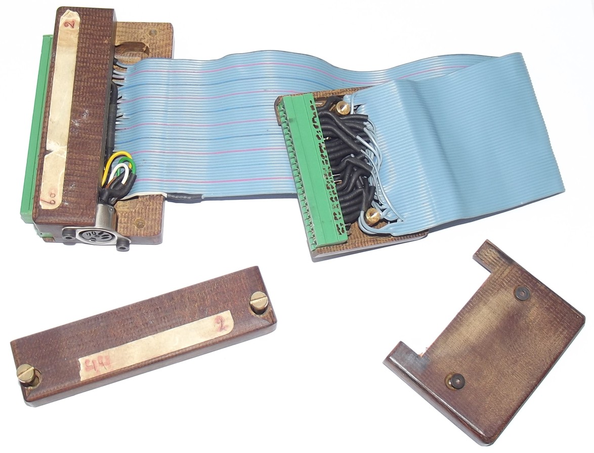
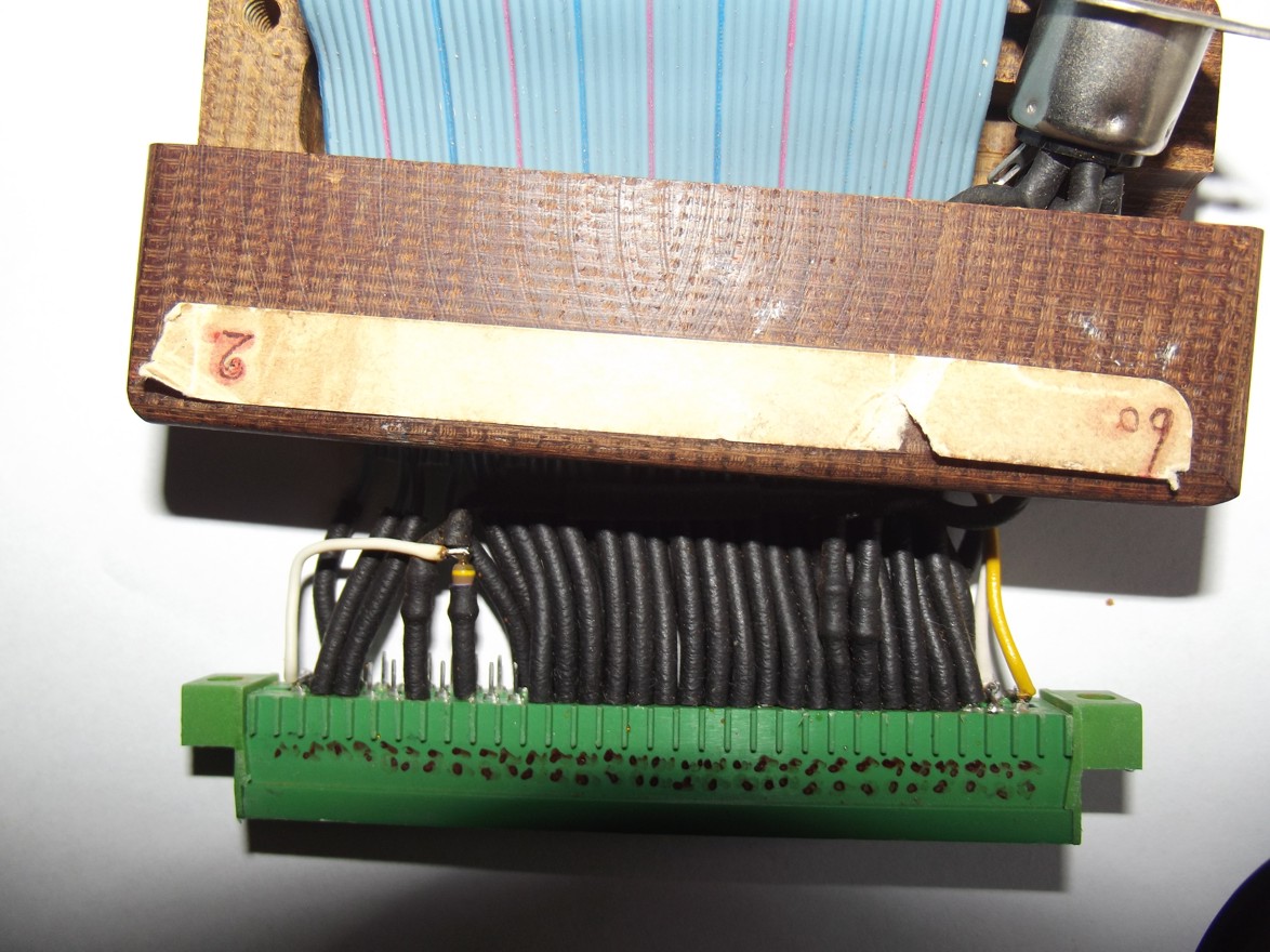
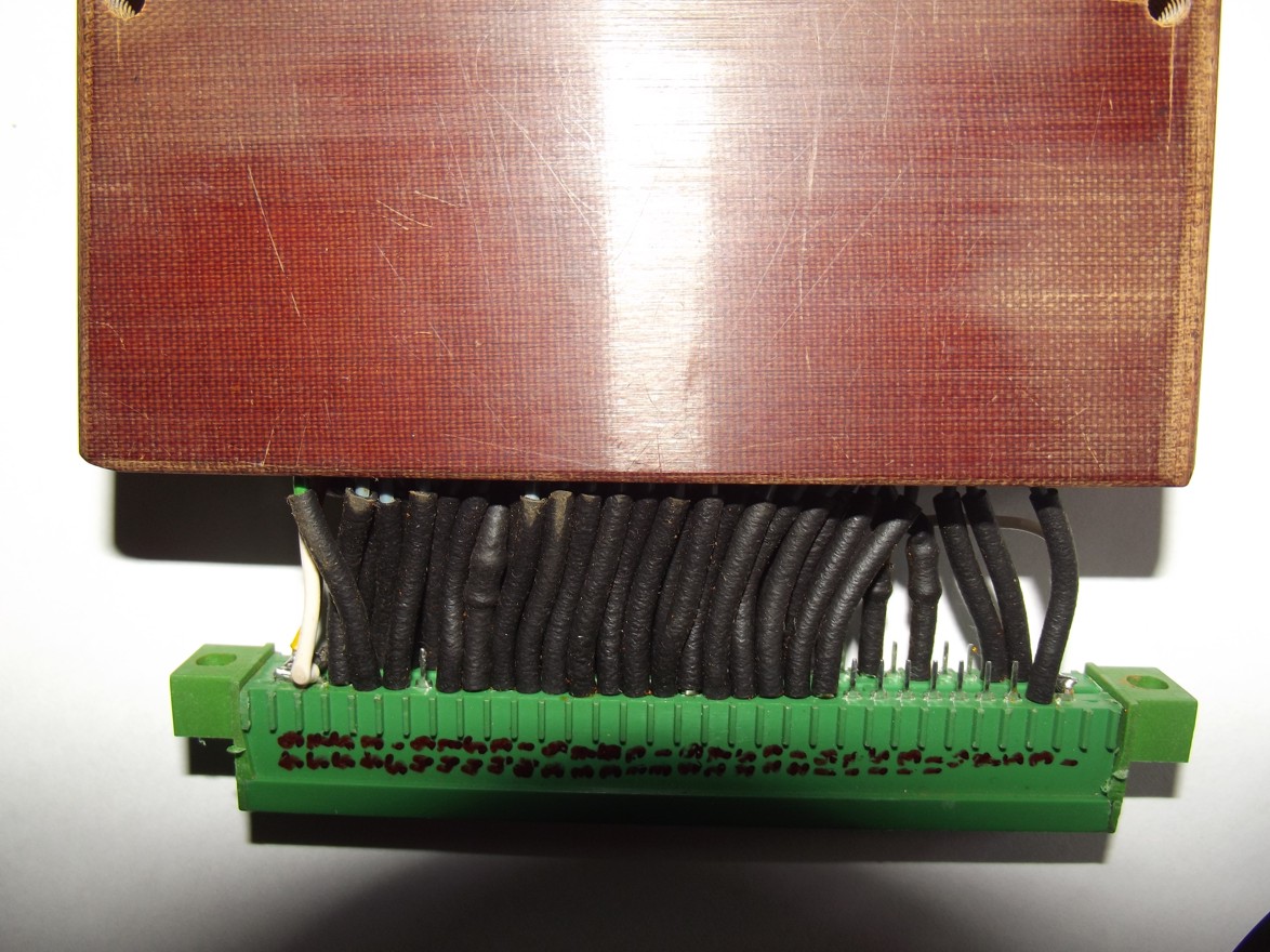