Mini-Cortex System
![]() Description
Description
![]() Specification
Specification
![]() Parts List
Parts List
![]() Technical Description
Technical Description
![]() Processor - General
Processor - General
![]() CRU Clock and External Instruction Decoding
CRU Clock and External Instruction Decoding
![]() Memory Wait State Generation
Memory Wait State Generation
![]() Single-Step Functionality
Single-Step Functionality
![]() CRU Control Signal Latch
CRU Control Signal Latch
![]() GAL Logic and Memory Maps
GAL Logic and Memory Maps
![]() Memory Mapper
Memory Mapper
![]() EEPROM and RAM
EEPROM and RAM
![]() Compact Flash Card
Compact Flash Card
![]() Serial Interface
Serial Interface
![]() Video Display Processor Interface
Video Display Processor Interface
![]() Power Supply and Power LED
Power Supply and Power LED
![]() References
References
![]() EEPROM, GAL and CF Card Images
EEPROM, GAL and CF Card Images
![]() Powering On and Boot Menu (using EEPROM Image 1)
Powering On and Boot Menu (using EEPROM Image 1)
![]() Using the EVMBUG Monitor (using EEPROM Image 1)
Using the EVMBUG Monitor (using EEPROM Image 1)
![]() Using Cortex BASIC (using EEPROM Image 1)
Using Cortex BASIC (using EEPROM Image 1)
![]() Using the Marinchip Disk Executive (MDEX) (using EEPROM Image 1)
Using the Marinchip Disk Executive (MDEX) (using EEPROM Image 1)
![]() Using Unix (using EEPROM Image 1)
Using Unix (using EEPROM Image 1)
![]() Unix Ports
Unix Ports
![]() Writing and Editing a Text File
Writing and Editing a Text File
![]() Compiling a C Program
Compiling a C Program
![]() Miscellaneous Unix Notes
Miscellaneous Unix Notes
![]() Programming Examples
Programming Examples
![]() Setting/Resetting a Bit in the CRU Control Signal Latch
Setting/Resetting a Bit in the CRU Control Signal Latch
![]() Memory Mapper
Memory Mapper
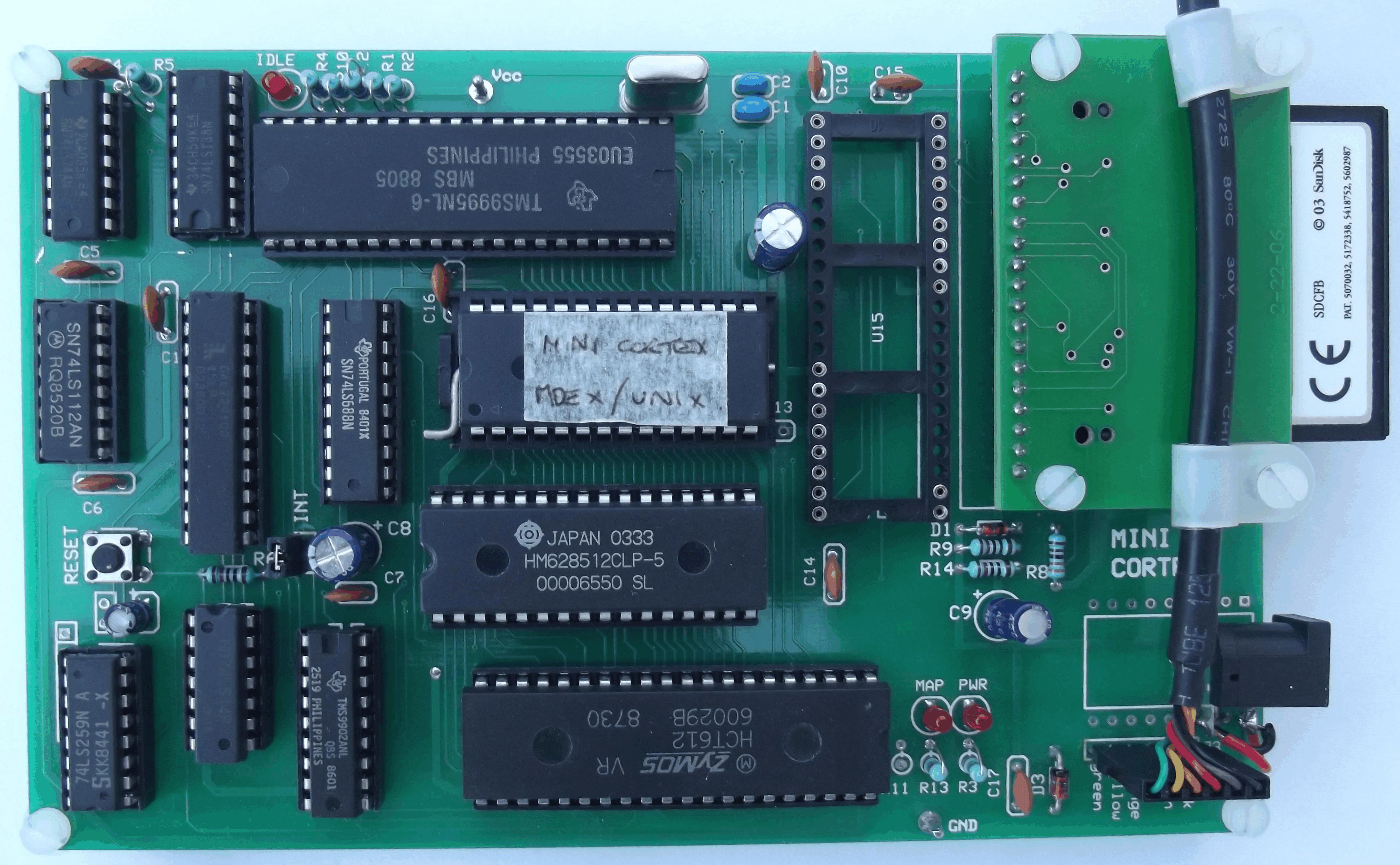 |
The Mini-Cortex system is a further development of my
TMS 9995 breadboard project to produce a system similar to a
Powertran Cortex, but using more modern components. The system design and PCB layout is the work of Paul Ruizendaal, with a little input from myself and a couple of others. The system is based around a TMS 9995 running at 3 MHz, with 32K byte EEPROM, 512K byte RAM accessed through a memory mapper, a serial port, a socket to interface a Compact Flash memory card, and a socket to fit an F18A video board (a pin-compatible replacement for the TMS 9918A, 9928, and 9929 video display processors). Two EEPROM images are available to support this system: EEPROM 1 provides a boot menu which enables the user to select between the EVMBUG system monitor from TI's TMS 9995 Evaluation Module, a port of the Powertran Cortex Power BASIC made for my TM 990 computer, the Marinchip Disk Executive (MDEX) operating system, and perhaps most interesting, an implementation of V6 Unix including a C compiler. EEPROM 2 provides a version of BASIC that is closer to the original Cortex BASIC, which provides better support for the Mini-Cortex hardware. |
The project requires the parts listed in the table below. All ICs are dual-inline packages. Capacitor voltages can be the specified value or greater.
| Circuit Diagram Reference | Description |
| U1 | TMS 9995 microprocessor, 12 MHz |
| U2 | 74LS612 or 74HCT612 memory mapper IC |
| U3 | 74LS14 hex Schmitt trigger inverter IC |
| U4 | AT28C256 256K bit, 32K x 8 EEPROM, 120ns or faster |
| U5 | 628512 4M bit, 512K x 8 RAM, 70ns or faster (Hitachi HM628512ALP or BLP, 70ns or 50ns works) |
| U6 | 74LS688 8-bit comparator IC |
| U7 | Compact Flash card breakout board. (Originally used one of these BOB-CFCARD which is now unavailable. I can provide a compatible board as a separate purchase, or a circuit diagram for interfacing an alternative MIKROE-76 Compact Flash interface board is included in this section if you want to do it yourself.) |
| U8 | TMS 9902ANL asynchronous communications controller |
| U9 | BOB-FT232R USB-to-serial interface board, or use a USB TTL serial cable similar to this connected to J3 |
| U10 | 74LS259 8-bit latch IC |
| U11 | GAL22V10D programmable GAL IC (programming equations are included below) |
| U12 | 74LS74 dual D-type flip-flop IC |
| U13 | 74LS112 dual J-K flip-flop IC |
| U14 | 74LS138 3-to-8 line decoder IC |
| U15 | F18A video board (optional) (on the V1 PCB, a 4.7pF capacitor also required to fix a bug in the circuit; this is C18 on the V2 PCB) |
| R1, R2, R4, R5, R6, R9, R10, R11, R14 (R11 fitted to V1 PCB only) |
10K metal film 0.6W resistor |
| R3, R12, R13 | 2K2 metal film 0.6W resistor |
| (R7 not used) | |
| R8 | 3K3 metal film 0.6W resistor |
| C1, C2 | 15pF ceramic capacitor |
| C3 | 1μF electrolytic capacitor, 16V |
| C4 - C7, C10, C12 - C17 | 0.1μF ceramic decoupling capacitor |
| C8, C11 | 100μF electrolytic capacitor, 16V |
| C9 | 10μF electrolytic capacitor, 16V |
| C18 (fitted to V2 PCB only) | 4.7pF ceramic capacitor |
| D1 | 1N914 diode |
| D2, D4, D5 | 3mm, low power (2mA) LED |
| D3 | 5V6 1.3W Zener diode |
| X1 | 12 MHz crystal (AEL Crystals part # X12M000000L188 works) |
| SW1 | Single pole, push-to-make, PCB mount, non-locking switch |
| J2, J3 | 6-pin SIL header |
| - | Jumper pins for RESET and INT jumpers |
| - | IC sockets to suit. A compact low profile ZIF socket can be used for the EEPROM U4 if it is likely to be removed often for reprogramming (on the V1 PCB, C13 may have to be omitted to fit the ZIF socket). I found that this one fits, which I believe to be a now-obsolete WELCON 630-7281612. You'll probably only find it under that part name/number at surplus stockists, but try a search on eBay for "low profile 28-pin ZIF socket" and look at the pictures for the socket with the distinctive "WE" logo. A machined pin socket is recommended for the F18A video board U15, with the socket cut to size (or non-used pins removed) as required. |
| - | Low profile male/female header for BOB-CFCARD U7 |
| PCB | Contact me for availability |
A circuit diagram for the project is available here (for the V2 PCB). Note that:
Processor U1 derives its clock from 12 MHz crystal X1. The crystal frequency is internally divided by 4 to give a processor clock speed of 3 MHz.
Processor interrupt /INT1 is not used in the system, so is tied high by resistor R1. Interrupt /INT4_/EC can be optionally connected to the TMS 9902 Asynchronous Communications Controller (ACC) U8 /INT output by fitting the INT jumper, and is otherwise pulled high by resistor R2. (The INT jumper is required to be fitted to run the Unix software described on this page; for the other software packages described, the jumper may be either fitted or not fitted.)
Direct memory access (DMA) by external devices is not used in the system so the processor /HOLD input is tied high by resistor R4.
Resistor R6 and capacitor C3 form a power-up reset circuit, with switch SW1 providing manual reset capability. The 2-pin jumper RESET enables a remote manual reset switch to be connected to the board. Schmitt trigger inverters U3a and U3b provide non-inverted and inverted reset signals which are fed to various parts of the circuit.
3-to-8 line decoder U14 is used to:
The external instructions used by the system are:
J-K bistable U13b controls memory wait state generation. After a system reset, when /RESET goes through a low-to-high transition, the bistable Q output and therefore the processor READY input is low, which disables the processor 'automatic first wait state generation' feature. From that point:
J-K bistable U13a and D-type bistables U12b and U12a implement the hardware side of the processor single-step functionality. The bistable are put in the 'set' state by a system reset. This sets the processor /NMI (Non-Maskable Interrupt) to the inactive high state. The bistables remain in this state when clocked by the IAQ (Instruction Acquisition) signal until an LREX instruction is executed which resets U13a. This pulses the U13a Q output low for the duration of one instruction. U12b and U12a delay this low pulse for a further two IAQ cycles and the pulse then causes a processor /NMI interrupt which forces an interrupt with the trap vector (workspace pointer and program counter) in memory words >FFFC and >FFFE.
The single-step functionality also requires software support. Prior to being used, memory words >FFFC and >FFFE have to be loaded with the workspace pointer and program counter for the code to run after the single-step operation - this is typically code in the monitor program to print the values of the processor registers. To execute a single step, the LREX instruction is executed, followed by a RTWP (Return from subroutine) where the vectors have been set to point to the instruction in the user's program to execute. In conjunction with the hardware, the LREX instruction triggers the single-step circuit; the RTWP instruction then a further single instruction in the user's program are executed, then the /NMI generated causes a return to the monitor program.
8-bit addressable latch U10 is mapped into the CRU map at addresses >0040 - >004E (with these addresses repeating up to >007F). Each latch output can be set high or low individually over the CRU interface. All the outputs are set to low on a system reset. The latch outputs are used as described in the table below.
Examples for addressing a specific bit in the latch using various languages/monitors are given here.
| Latch Output | CRU Address | Function |
| Q0 (/ROMEN) | >0040 | Set to low to enable access to the ROM, and high to disable access. When disabled, RAM is mapped into the ROM address space. |
| Q1 (MAPEN) | >0042 | Set to high to enable the memory mapper, and low to disable. |
| Q2 (USER) | >0044 | Set to high to set 'user mode' in the Unix operating system. In this mode, access to the CF card, the memory mapper registers and the TMS 9902 is blocked, and write protection of memory blocks in RAM is enabled. (A user program can always reset the bit, so it does not protect from malicious code, but should help as a minor defense against bugs taking the system down.) |
| Q3 - Q7 | >0046 - >004E | Spare. Routed to connector J2 for use by the user if required. |
GAL U11 performs the majority of the signal decoding in the system. Using a GAL not only considerably reduces the chip count, it also reduces the signal decoding delay to just 15ns.
The GAL output equations are shown in the circuit diagram and explained in the table below. Several of the inputs to the GAL require particular explanation:
| Signal | Equation ('+' is 'OR', '*' is 'AND') | Logic |
| /ROMSEL | /MEMEN+/ROMEN+RA15 | /ROMSEL is active (low) to access the ROM when: • /MEMEN is low, indicating a memory access cycle, and • /ROMEN is low (default state at power-up), and • RA15 is low, indicating a memory access in the address range >0000 - >7FFF. |
| /RAMSEL | /MEMEN+!/ROMEN*!RA15*/WE+!/ISFE*RA15 | (* AND operator takes precedence over + OR
operator, so the equation is effectively:
/MEMEN+(!/ROMEN*!RA15*/WE)+(!/ISFE*RA15) /RAMSEL is active (low) to access the RAM when: • /MEMEN is low, indicating a memory access cycle, and either • /ROMEN, RA15 and /WE are low, indicating a write cycle in the address range >0000 - >7FFF when ROM is enabled, or • /ISFE and RA15 are high, indicating a memory access in the range >8000 - >FFFF excluding the range >FExx. The middle part of the equation involving /ROMEN, RA15 and /WE enables writing 'under' the ROM to RAM - that is, you can read each address in the ROM, write the data back to the ROM whereby it gets written to RAM (and so creating an image of the ROM in RAM), then disable the ROM and continue running from RAM. |
| /CFSEL | /MEMEN+/ISFE+!RA15+AB7+AB6+USER | /CFSEL is active (low) to access the CF
card when: • /MEMEN is low, indicating a memory access cycle, and • /ISFE is low, indicating a memory access in the range >FExx, and • RA15 is high, indicating a memory access in the range >8000 - >FFFF, and • AB7 and AB6 (processor address bits A8 and A9) are both low, indicating a memory access in the range >xx00 - >xx3F, and • USER is low. |
| /MAPSEL | /MEMEN+/ISFE+!RA15+AB7+!AB6+USER | /MAPSEL is active
(low) to access the memory mapper when: • /MEMEN is low, indicating a memory access cycle, and • /ISFE is low, indicating a memory access in the range >FExx, and • RA15 is high, indicating a memory access in the range >8000 - >FFFF, and • AB7 (processor address bit A8) is low and AB6 (processor address bit A9) is high, indicating a memory access in the range >xx40 - >xx7F, and • USER is low. |
| /PWE | /WE+PROTECT*USER | /PWE (Protected Write Enable) is active (low) when: • /WE is low, indicating a memory write cycle, and either • PROTECT is low, or • USER is low. (Conversely, generation of an active low /PWE signal is inhibited when PROTECT and USER are both high. /PWE is fed to the RAM, CF card and memory mapper. As the 'chip enable' signals for the CF card and memory mapper are both disabled when USER is high, write protection is in effect only functional on the RAM; the state of PROTECT is irrelevant for the CF card and memory mapper as they are disabled by the high USER signal.) |
| /9902SEL | !/MEMEN+/ISFE+RA15+AB7+AB6+USER | /9902SEL is active (low) to access the
TMS9902 when: • /MEMEN is high, indicating a CRU cycle, and • /ISFE is low, indicating a CRU access in the range >00xx, and • RA15 is low (as it will be as it is not used for CRU operations), and • AB7 and AB6 (processor address bits A8 and A9) are both low, indicating a memory access in the range >xx00 - >xx3F, and • USER is low. |
| WAIT | !/ROMSEL+!/CFSEL | WAIT is active (high)
to add a single-wait state to a memory access when: • /ROMSEL is low (ROM is being accessed), or • /CFSEL is low (the CF card is being accessed). |
| /FLAGSEL | /CRUCLK+/ISFE+RA15+AB7+!AB6 | /FLAGSEL is active (low) to write CRU data
to the control signal latch U10 when: • /CRUCLK is low, and • /ISFE is low, indicating a CRU access in the range >00xx, and • RA15 is low (as it will be as it is not used for CRU operations), and • AB7 (processor address bit A8) is low and AB6 (processor address bit A9) is high, indicating a memory access in the range >xx40 - >xx7F. |
| /CSR | /MEMEN+/ISFE+!RA15+!AB7+AB6+USER+/DBIN | /CSR is active (low)
to read from the VDP when: • /MEMEN is low, indicating a memory access cycle, and • /ISFE is low, indicating a memory access in the range >FExx, and • RA15 is high, indicating a memory access in the range >8000 - >FFFF, and • AB7 (processor address bit A8) is high and AB6 (processor address bit A9) is low, indicating a memory access in the range >xx80 - >xxFF, and • USER is low, and • /DBIN is low, indicating a memory read cycle. |
| /CSW | /MEMEN+/ISFE+!RA15+!AB7+AB6+USER+/WE | /CSW is active (low) to write to the VDP
when: • /MEMEN is low, indicating a memory access cycle, and • /ISFE is low, indicating a memory access in the range >FExx, and • RA15 is high, indicating a memory access in the range >8000 - >FFFF, and • AB7 (processor address bit A8) is high and AB6 (processor address bit A9) is low, indicating a memory access in the range >xx80 - >xxFF, and • USER is low, and • /WE is low, indicating a memory write cycle. |
The memory map is shown in the table below.
| Memory Address | Mapped To |
| >0000 - >7FFF | ROM when enabled, otherwise RAM |
| >8000 - >EFFF | RAM |
| >F000 - >F0FB | TMS 9995 internal RAM |
| >F0FC - >FDFF | RAM |
| >FE00 - >FE3F | CF card ATA registers |
| >FE40 - >FE7F | Memory mapper registers 0-15 (>FE40 – >FE4F, repeats at >FE50 etc.) |
| >FE80 - >FEBF | VDP registers (when VDP fitted) |
| >FEC0 - >FFF9 | RAM |
| >FFFA - >FFFF | TMS 9995 internal RAM |
The CRU map is shown in the table below.
| CRU Address | Mapped To |
| >0000 - >003F | TMS 9902 registers |
| >0040 - >007F | Control signal latch (further details here) |
| (Plus processor internal CRU bits) |
In memory mapper U2, the four most significant bits of the processor address bus select one of 16 map registers that contain 12 bits each. In this system, 7 of these 12 bits along with the other bits of the processor address bus are used to address the 512K byte RAM. By loading and reloading the map registers as required, any 4K byte block of the processor 64K byte memory space can be mapped to any 4K byte block in the 512K byte RAM.
The memory mapper has four modes of operation: read, write, map and passthrough.
The memory mapper is in read or write mode when /CS is low. /CS is connected to the /MAPSEL output of the GAL.
In read or write mode, data can be read from or loaded into the map register selected by the processor least significant address lines A12 - A15 via the mapper register select inputs RS0 - RS3 under the control the R/W input (read is active high, write is active low). Writes to the map registers also require the /STROBE input to be low. The data I/O takes place over the processor data bus. (The way in which the processor data bus D0 - D7 is split between the memory mapper data bits D1 - D4 and D8 - D11 has no significance other than making the signal routing on the PCB slightly easier. The connection of processor data line D4 to multiple data inputs on the mapper is due to a small design change from the V1 PCB where minimal changes to the PCB layout were desired.)
The memory mapper registers are mapped to the processor memory address range >FE40 - >FE4F (so >FE40 is map register 0, >FE41 is map register 1, and so on).
Map mode is active when the /CS input is high and /MM (map mode control) is low. /MM is connected to the MAPEN output of the CRU control signal latch U10 (described here) via inverter U3c. When map mode is active, the MAP LED D5 is illuminated.
In map mode, processor most significant address lines A0 - A3 select one of the 16 map registers via the mapper MA0 - MA3 inputs. The 12 bits of the map register are output on the mapper MO0 - MO11 outputs. Mapper outputs MO8 - MO11 and MO1 - MO3 form system address bus bits AB12 - AB18 which are used only by the RAM.
Mapper output MO4 is not used for addressing but forms the PROTECT signal which is an input to the GAL. Setting this bit in a map register inhibits generation of the /WE signal to the RAM when that memory block is accessed and the system is running in 'user mode'.
Passthrough mode is active when the /CS and /MM inputs are both high. In this mode, the address bits on the MA0 - MA3 inputs are presented on the MO8 - MO11 outputs. This is the default mode after a system reset, and it effectively bypasses the memory mapper.
A passthrough map is a set of map register values where the same 4K byte block in RAM is accessed for each of the 4K byte blocks in the processor 64K byte memory space when the mapper is enabled, as when the mapper is not enabled. These map register values are typically written to the map registers before the mapper is enabled so that the processor continues accessing and running the same software immediately after the mapper is enabled. In this system, the passthrough map is >00 (written to map register 0), >08, >01, >09, >02, >0A, >03, >0B, >04, >0C, >05, >0D, >06, >0E, >07 and >0F (written to map register 15). These values are derived as described below.
Processor most significant address bits A0 – A3 are fed to the mapper MA3 – MA0 inputs as shown in the first table below, and in passthrough mode are presented on the mapper MO11 – MO8 outputs as shown. To load a passthrough map into the mapper, the map registers have to be loaded with the same bit patterns as on A0 – A3. These bits of the map registers are loaded from processor data bus bits D4 - D7 as shown in the table, but note that processor data bit D4 is out of sequence, and this affects the data byte that has to be written to correspond to a particular bit pattern on A0 - A3.
The second table below lists each of the 4K byte blocks in the processor 64K byte memory space, the value of A0 - A3 for each block, the map register that is loaded to map that block to a particular memory block in RAM, and the bit pattern needed on D4 - D7 to match the bit pattern on A0 - A3 (in effect, the bit pattern needed on D4 – D7 is obtained by moving address bit A3 from the far right to the far left, before bits A0 – A2; so for example 0001 becomes 1000, and 0011 becomes 1001. ). This last column is the passthrough map value for each map register.
| Processor Address Bit | Input to Mapper | Output From Mapper in Passthrough Mode |
Loaded from Processor Data Bit |
| A0 (MSb) | MA3 | MO11 | D5 |
| A1 | MA2 | MO10 | D6 |
| A2 | MA1 | MO9 | D7 |
| A3 (LSb) | MA0 | MO8 | D4 |
| 4K Block Address (Hex) |
A0 ... A15 (Binary) |
A0 - A3 Address Map Register | Bit Pattern Needed on D4 - D7 to Match Bit Pattern on A0 - A3 |
| >0xxx | 0000 xxxx xxxx xxxx | 0 | 0000 - 0 |
| >1xxx | 0001 xxxx xxxx xxxx | 1 | 1000 - 8 |
| >2xxx | 0010 xxxx xxxx xxxx | 2 | 0001 - 1 |
| >3xxx | 0011 xxxx xxxx xxxx | 3 | 1001 - 9 |
| >4xxx | 0100 xxxx xxxx xxxx | 4 | 0010 - 2 |
| >5xxx | 0101 xxxx xxxx xxxx | 5 | 1010 - A |
| >6xxx | 0110 xxxx xxxx xxxx | 6 | 0011 - 3 |
| >7xxx | 0111 xxxx xxxx xxxx | 7 | 1011 - B |
| >8xxx | 1000 xxxx xxxx xxxx | 8 | 0100 - 4 |
| >9xxx | 1001 xxxx xxxx xxxx | 9 | 1100 - C |
| >Axxx | 1010 xxxx xxxx xxxx | 10 | 0101 - 5 |
| >Bxxx | 1011 xxxx xxxx xxxx | 11 | 1101 - D |
| >Cxxx | 1100 xxxx xxxx xxxx | 12 | 0110 - 6 |
| >Dxxx | 1101 xxxx xxxx xxxx | 13 | 1110 - E |
| >Exxx | 1110 xxxx xxxx xxxx | 14 | 0111 - 7 |
| >Fxxx | 1111 xxxx xxxx xxxx | 15 | 1111 - F |
Some examples of programming the memory mapper are given here.
32K byte EEPROM U4 is connected directly to the processor address and data buses. The EEPROM /OE (Output Enable) input is connected to the processor /DBIN output, which when active low indicates that the processor has disabled its data bus output buffers to allow external memory to output data onto the data bus. The /CE (Chip Enable) input is the /ROMSEL output from the GAL; how this signal is generated and the location of the EEPROM in the processor memory map is described here. ROM is enabled when the /ROMEN output of the CRU control signal latch is low. When /ROMEN is high, RAM is mapped to the ROM address space.
512K byte RAM U5 is addressed by the lower 12 bits of the processor address bus and the 7 bits from the memory mapper. The RAM /OE input is connected to the processor /DBIN output in the same way as the EEPROM. The /CS (Chip Select) input is the /RAMSEL output from the GAL. The /WE (Write Enable) input is the /PWE (Protected Write Enable) output from the GAL.
The CF Card plugs into a breakout board ('BOB') fitted to the PCB.
The CF card is used for disk storage emulation for the MDEX and Unix software, which read and write to the card using the FAT32 format so disk images can be loaded onto the card direct from a PC. The card operates in memory mode and with an 8-bit data bus rather than the 16-bit data bus used in true IDE mode. Communication with the card is through a set of 8-bit registers, with data transfers occurring in 512-byte blocks. The three address inputs, connected to the processor three least significant address bits, enable selection of the eight registers. The /CE input is the /CFSEL output from the GAL; how this signal is generated and the location of the CF card in the processor memory map is described here.
In the power supply circuit, diode D1 drops the supply voltage to the CF card by 0.7V to ensure that the logic levels used by the CF card are within the range used by the TMS 9995. Pullup resistors R9, R10 and R14 further improve the logic level voltage matching.
The original breakout board (BOB-CFCARD) used with the system is now unavailable. A compatible board is available as a separate purchase, or as an alternative, a MIKROE-76 Compact Flash interface board can be interfaced to the BOB connector as shown in this circuit diagram.
TMS 9902 Asynchronous Communications Controller (ACC) U8 is a CRU peripheral device which provides the interface between the processor and a serial, asynchronous, RS-232 communications channel. The /CE input is the /9902SEL output from the GAL; how this signal is generated and the location of the TMS 9902 in the processor CRU map is described here. Jumper INT enables the TMS 9902 /INT (interrupt) output to be fed to or isolated from the processor /INT4 input.
The TMS 9902 send data (XOUT) and receive data (RIN) signals are connected to U9 (an optional USB-to-serial bridge breakout board) and connector J3 (which enables connection of an external USB TTL serial cable).
IC position U15 is for an optional F18A video board, which is an FPGA implementation of the TMS 9918 video display processor (VDP) with a VGA output. The VDP /CSR (Chip Select Read) and /CSW (Chip Select Write) inputs are generated by the GAL; how these signals are generated and the location of the VDP in the processor memory map is described here.
For the F18A to work properly on a V1 PCB, it has been found necessary to fit a ~4.7pF ceramic capacitor on the underside of the PCB between pins 13 (MODE) and 12 (GND). (This capacitor is incorporated into the V2 PCB as C18.)
The only software application that currently supports the VDP is Cortex BASIC.
The board is powered from a single +5V regulated supply, intended to be connected through the USB-to-serial bridge breakout board. If this breakout board is not used, power can be supplied through connector J3 or a separate power connector can be fitted to suit the user's requirements. Zener diode D3 provides reverse polarity protection.
Capacitors C8, C11 and C9 provide power supply smoothing. The supply to individual ICs is decoupled by capacitors C4 - C7, C10 and C12 - C17.
PWR LED D2 in series with current limiting resistor R3 provides a visual indication that power is applied.
TMS 9995 processor data manual
74LS612 memory mapper IC data sheet
74LS14 hex Schmitt trigger inverter IC data sheet
AT28C256 256K bit, 32K x 8 EEPROM data sheet
628512 4M bit, 512K x 8 RAM data sheet
74LS688 8-bit comparator IC data sheet
BOB-CFCARD Compact Flash card breakout board catalogue page
TMS 9902ANL asynchronous communications controller data sheet
BOB-FT232R USB-to-serial interface board catalogue page
74LS259 8-bit latch IC data sheet
GAL22V10D programmable GAL IC data sheet
74LS74 dual D-type flip-flop IC data sheet
74LS112 dual J-K flip-flop IC data sheet
74LS138 3-to-8 line decoder IC data sheet
F18A video board catalogue entry
TMS 9918 video display processor data manual
EEPROM 1 (EVMBUG, port of Cortex BASIC, MDEX, Unix) - EEPROM image here.
EEPROM 2 (Cortex BASIC) - EEPROM image here. This version of Cortex BASIC is closer to that in the original Powertran Cortex (whereas the version above is a port to work with the TMS 9900), and provides better support for the Mini-Cortex hardware such as the memory mapper. This version defaults to communicating over the RS-232 port (19200 Baud, 7 data bits, even parity, 2 stop bits).
GAL JEDEC programming file here.
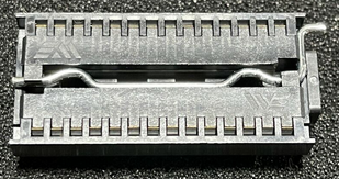
The CF card has to be newly formatted with an MBR (master boot record), a single partition formatted as FAT32, and a cluster size of 4096 bytes - the CF card needs to be at least 256 MB to support this. Not all brands/sizes of CF card seem to work - you may have more success with an older, low capacity card. A SanDisk 2.0GB card with a "SDCFB" marking on the back (photo here) works well.
It can be problematic formatting a new card using Windows 10 as it does not always seem to write an MBR to the card. I use a formatting utility called Rufus (details and download here) with these settings. Once the card is correctly formatted, use Windows to write the four files here directly to the card.
The serial port on the Mini-Cortex is configured for 9600 Baud, 7 data bits, even parity, one stop bit, no flow control.
The EVMBUG monitor and Cortex BASIC software applications, and the boot loaders for MDEX and Unix, are stored on a single 32K byte EEPROM. The required application is selected from a boot menu. To display the boot menu, connect the Mini-Cortex to a configured serial port on a PC, apply power to the Mini-Cortex, then press any key.
TMS 9995 BREADBOARD SYSTEM
BY STUART CONNER
PRESS 1 FOR EVMBUG MONITOR
PRESS 2 FOR CORTEX BASIC
PRESS 3 FOR MDEX
PRESS 4 FOR UNIX
To select a software application from the menu, press the corresponding numeric key.
The EVMBUG system monitor is from TI's TMS 9995 Evaluation Module. It provides an interactive interface between the user and the system. EVMBUG is described on this page. Note that the 'SS' single step command is supported by the Mini-Cortex hardware.
When EVMBUG is selected from the boot menu, the code is copied from the EEPROM to RAM at >8000 and then run from RAM.
TMS 9995 BREADBOARD SYSTEM
BY STUART CONNER
PRESS 1 FOR EVMBUG MONITOR
PRESS 2 FOR CORTEX BASIC
PRESS 3 FOR MDEX
PRESS 4 FOR UNIX
(Press 1)
EVMBUG R1.0
MON?
The tag format loader LMC command can be used to download a program assembled using the Asm99/4a assembler on the PC. A utility is required on the PC to feed the program object code to the serial port - details TBD.
The BASIC interpreter is based on a port of the Powertran Cortex Power BASIC made for my TM 990 computer.
Cortex BASIC is designed to run from RAM, so to avoid having to rewrite and restructure sections of the code for the Mini-Cortex project, when Cortex BASIC is selected from the boot menu the code is copied from the EEPROM to RAM at >8000 and then run from RAM. This leaves only about 3K bytes of memory free for program storage - but this should be sufficient for 'tinkering' considering that there is currently no means of saving a program.
TMS 9995 BREADBOARD SYSTEM
BY STUART CONNER
PRESS 1 FOR EVMBUG MONITOR
PRESS 2 FOR CORTEX BASIC
PRESS 3 FOR MDEX
PRESS 4 FOR UNIX
(Press 2)
-- TMS 9995 BREADBOARD BASIC Rev. 1.1 --
[Ported from Cortex BASIC (C)1982 by Stuart Conner]
*Ready
The Cortex BASIC user guide is available here.
Mapping between the keys on the Cortex computer and the keys on the PC keyboard is as shown in the following table.
| Cortex Key | PC Keyboard Key |
| Enter | Return |
| Edit | Ctrl-T |
| Clear | Ctrl-L |
| Escape | Esc |
| Graphic | (not supported) |
| Insert | Ctrl-V |
| Delete | Ctrl-C |
| Rubout | Backspace |
| Cursor Up | Ctrl-E |
| Cursor Down | Ctrl-X |
| Cursor Left | Ctrl-S |
| Cursor Right | Ctrl-D |
| Home | Ctrl-H |
When BASIC is in use, all keyboard input is automatically converted to upper case.
The graphics commands are supported by the F18A VDP, when fitted.
There are some changes and restrictions in the Mini-Cortex implementation as compared to the implementation described in the Cortex user guide:
The Marinchip Disc Executive (MDEX) is a complete operating system from Marinchip Systems that ran on their M9900 system. A Cortex version was made available by Micro Processor Engineering (Southampton, UK) which, once loaded, completely replaces Cortex BASIC and provides a rich programming and development environment. Several languages are available (QBASIC, SPL, Pascal, Forth, Assembler), along with a professional Word Processor.
MDEX documentation is available on the site http://www.powertrancortex.com/documentation.html. The documentation and MDEX disks were recovered and made available by Dave Hunter, the owner of the www.powertrancortex.com site. Porting of the MDEX files to the Mini-Cortex was by Paul Ruizendaal. On the Mini-Cortex, the files are stored in two emulated disks on the CF card.
Note that the start of the "Marinchip Disc Executive (Ver. SDJ 1.0)" line in the boot sequence below is sometimes a bit garbled - possibly a bug with resetting the TMS 9902 which loses sync. It is OK after that though.
TMS 9995 BREADBOARD SYSTEM
BY STUART CONNER
PRESS 1 FOR EVMBUG MONITOR
PRESS 2 FOR CORTEX BASIC
PRESS 3 FOR MDEX
PRESS 4 FOR UNIX
(Press 3)
>>>>>>
Marinchip Disc Executive (Ver. SDJ 1.0)
.
.dir
. 120 0 BOOT$ .SAV 100 120 SHELL$ .OBJ 44 220
ASM 114 264 BASIC 214 378 BRAINS 26 592
CAT 16 618 PAUL .TXT 10 634 CFDISC .ASM 138 3345
CONFIG .ASM 20 769 CONFIG .REL 10 789 COPY 26 799
CRU-CORTEX 20 825 DEBUG 18 845 DISASM 56 863
DISC .REL 36 919 DRIVECON 52 955 DU 30 1007
EDIT 112 1037 FDIAG 12 1149 LINK 56 1161
MDEX .REL 150 1217 MDEX02PP.LNK 10 1367 PACK 106 1377
PPRINT .ASM 200 1483 PPRINT .REL 8 1683 SIZE 10 1691
SWAP 2 1701 SYSDEF 10 1703 TEMP1$ 450 1713
TEMP2$ 450 2163 TERM9902.ASM 90 2613 TERM9902.REL 50 2703
TYPE 10 2753 WINDOW 350 2763 WORD 96 3113
Sectors available 7500. Largest block: 4799
.
Porting of Unix to the Mini-Cortex has been done in two stages, both by Paul Ruizendaal:
TMS 9995 BREADBOARD SYSTEM
BY STUART CONNER
PRESS 1 FOR EVMBUG MONITOR
PRESS 2 FOR CORTEX BASIC
PRESS 3 FOR MDEX
PRESS 4 FOR UNIX
(Press 4)
>>>>>
Mem.......512KB
login: root
# cd ../../bin
# ls -l
total 1591
-rwxr-xr-x 1 root 9918 Dec 28 11:50 ac
-rwxr-xr-x 1 root 11442 Dec 28 11:50 ar
-rwxr-xr-x 1 root 16416 Dec 28 11:50 as
-rwxr-xr-x 1 root 45508 Dec 28 11:50 awk
-rwxr-xr-x 1 root 1766 Dec 28 11:50 basename
-rwxr-xr-x 1 root 16410 Dec 28 11:50 bc
-rwxr-xr-x 1 root 6434 Dec 28 11:50 cal
-rwxr-xr-x 1 root 5346 Dec 28 11:50 cat
-rwxr-xr-x 1 root 9770 Dec 28 11:50 cc
-rwxr-xr-x 1 root 14398 Dec 28 11:50 cdb
-rwxr-xr-x 1 root 7782 Dec 28 11:50 chgrp
-rwxr-xr-x 1 root 5360 Dec 28 11:50 chk
-rwxr-xr-x 1 root 5122 Dec 28 11:50 chmod
-rwxr-xr-x 1 root 7768 Dec 28 11:50 chown
-rwxr-xr-x 1 root 6692 Dec 28 11:50 clri
-rwxr-xr-x 1 root 7018 Dec 28 11:50 cmp
-rwxr-xr-x 1 root 1900 Dec 28 11:50 col
-rwxr-xr-x 1 root 7062 Dec 28 11:50 comm
-rwxr-xr-x 1 root 850 Dec 28 11:50 cp
-rwxr-xr-x 1 root 19754 Dec 28 11:50 cpp
-rwxr-xr-x 1 root 2978 Dec 28 11:50 date
-rwxr-xr-x 1 root 27464 Dec 28 11:50 dc
-rwxr-xr-x 1 root 6446 Dec 28 11:50 dcheck
-rwxr-xr-x 1 root 9782 Dec 28 11:50 dd
-rwxr-xr-x 1 root 7944 Dec 28 11:50 df
-rwxr-xr-x 1 root 12600 Dec 28 11:50 diff
-rwxr-xr-x 1 root 6658 Dec 28 11:50 du
-rwxr-xr-x 1 root 344 Dec 28 11:50 echo
-rwxr-xr-x 1 root 9840 Dec 28 11:50 ed
-rwxr-xr-x 1 root 12250 Dec 28 11:50 egrep
-rwxr-xr-x 1 root 8066 Dec 28 11:50 fgrep
-rwxr-xr-x 1 root 9312 Dec 28 11:50 file
-rwxr-xr-x 1 root 11700 Dec 28 11:50 find
-rwxr-xr-x 1 root 9186 Dec 28 11:50 grep
-rwxr-xr-x 1 root 7750 Dec 28 11:50 icheck
-rwxr-xr-x 1 root 8338 Dec 28 11:50 idate
-rwxr-xr-x 1 root 5912 Dec 28 11:50 kill
-rwxr-xr-x 1 root 14002 Dec 28 11:50 ld
-rwxr-xr-x 1 root 33884 Dec 28 11:50 lex
-rwxr-xr-x 1 root 474 Dec 28 11:50 ln
-rwsr-xr-x 1 root 7436 Jan 08 14:26 login
-rwxr-xr-x 1 root 11772 Dec 28 11:50 ls
-rwsr-xr-x 1 root 11690 Dec 28 11:50 mail
-rwxr-xr-x 1 root 21828 Dec 28 11:50 make
-rwxr-xr-x 1 root 6706 Dec 28 11:50 man
-rwsr-xr-x 1 root 6802 Dec 28 11:50 mkdir
-rwxr-xr-x 1 root 6962 Dec 28 11:50 mv
-rwxr-xr-x 1 root 6808 Dec 28 11:50 ncheck
-rwsr-xr-x 1 root 9378 Dec 28 11:50 newgrp
-rwxr-xr-x 1 root 6378 Dec 28 11:50 nice
-rwxr-xr-x 1 root 7314 Dec 28 11:50 nm
-rwxr-xr-x 1 root 39952 Dec 28 11:50 nroff
-rwxr-xr-x 1 root 8878 Dec 28 11:50 od
-rwsr-xr-x 1 root 4356 Dec 28 11:50 passwd
-rwxr-xr-x 1 root 11126 Dec 28 11:50 pr
-rwsr-xr-x 1 root 7754 Dec 28 11:50 ps
-rwxr-xr-x 1 root 616 Dec 28 11:50 pwd
-rwxr-xr-x 1 root 17200 Dec 28 11:50 ratfor
-rwxr-xr-x 1 root 1680 Dec 28 11:50 reloc
-rwxr-xr-x 1 root 6032 Dec 28 11:50 rev
-rwxr-xr-x 1 root 6092 Dec 28 11:50 rm
-rwxr-xr-x 1 root 5980 Dec 28 11:50 rmdir
-rwxr-xr-x 1 root 6164 Dec 28 11:50 sh
-rwxr-xr-x 1 root 5666 Dec 28 11:50 size
-rwxr-xr-x 1 root 5038 Dec 28 11:50 sleep
-rwxr-xr-x 1 root 12630 Dec 28 11:50 sort
-rwxr-xr-x 1 root 6486 Dec 28 11:50 split
-rwxr-xr-x 1 root 6720 Dec 28 11:50 strip
-rwxr-xr-x 1 root 7114 Dec 28 11:50 stty
-rwxr-xr-x 1 root 6328 Dec 28 11:50 sum
-rwxr-xr-x 1 root 192 Dec 28 11:50 sync
-rwxr-xr-x 1 root 2192 Dec 28 11:50 tail
-rwxr-xr-x 1 root 21068 Dec 28 11:50 tar
-rwxr-xr-x 1 root 1444 Dec 28 11:50 tee
-rwxr-xr-x 1 root 7432 Dec 28 11:50 time
-rwxr-xr-x 1 root 5460 Dec 28 11:50 touch
-rwxr-xr-x 1 root 13398 Dec 28 11:50 tp
-rwxr-xr-x 1 root 2786 Dec 28 11:50 tr
-rwxr-xr-x 1 root 5354 Dec 28 11:50 tty
-rwxr-xr-x 1 root 5424 Dec 28 11:50 uname
-rwxr-xr-x 1 root 7030 Dec 28 11:50 uniq
-rwxr-xr-x 1 root 6552 Dec 28 11:50 wc
-rwxr-xr-x 1 root 4074 Dec 28 11:50 who
-rwxr-xr-x 1 root 29070 Dec 28 11:50 yacc
#
The Unix commands currently supported are shown in the directory listing above. The V6 Unix manuals are available at http://man.cat-v.org/unix-6th/. Note that the man pages provided directly on the Mini-Cortex (man <command>) are not always in sync with the actual binaries, and that several binaries in Cortex Unix have V7 extensions (or are actual V7 files).
To write a simple C program to a text file using the ed editor:
# ed -> runs the editor
a -> command to append text
#include <stdio.h>
int main() {
int count;
for(count=1;count<=10;count++)
printf("%d ",count);
printf("\n");
}
. -> returns to command mode
w test.c -> write file with specified name
111 ->
editor returns number of characters written
q -> quits the editor
#
-> back at the Unix prompt
To list the contents of the file from the Unix prompt:
# cat test.c
#include <stdio.h>
int main() {
int count;
for(count=1;count<=10;count++)
printf("%d ",count);
printf("\n");
}
#
To edit an existing file (editor shows number of characters in file after loading):
ed <filename>
Further ed commands, when in command mode (remember to type . to return to command mode after inserting or changing a line):
1,3l List the file from line 1 to line 3 (lowercase "L" at the end).
1,$l List the file from line 1 to the last line (lowercase "L" at the end).
<number> Set the addressed line to the specified line and list that line.
. List the line currently being addressed.
+ - Move the line pointer to the next or previous line, and lists that line.
i Insert a line before the line currently being addressed and enter insert mode.
<number>i Insert a line before the specified line and enter insert mode.
$i Insert a line at the end of the file and enter insert mode.
<number>d Delete the specified line.
d Delete the line currently being addressed.
<number>c Change (edit) the specified line and enter insert mode (retype the line).
c Change
(edit) the line currently being addressed and enter insert mode.
s/<this>/>that> Replace <this> with <that> throughout the file.
<number>s/<this>/>that> Replace <this> with <that> on the specified line only.
= Shows the line number of the currently addressed line.
Further information on the ed commands can be found by typing man ed at the Unix prompt.
To compile, assemble and link the C program in test.c to produce an executable file named test:
cc -O -o test test.c
where:
To compile, assemble and link the program as separate steps requires the following sequence of commands:
cc -S -O test.c
as -u -o test.o test.s
ld -X -o test
/lib/crt0.o test.o -L/lib -lc -lcrt
where:
Adding the -v option to the cc command to compile, assemble and link directly to an executable (that is, cc -O -v -o test test.c) lists the separate commands invoked during that operation.
The assembler produces a file that is set to start at location >0000 by default. On the Mini-Cortex, V6 binaries begin at location >1000. There are two ways to relocate: use the linker/loader ld or the special purpose program reloc. Both ld and cc accept the -a option to set the base address (for example, "-a 0x1000"). In the case of cc, if you don't specify any base address, the value 0x1000 is assumed. reloc accepts an octal relocation address. It is normally only used for assembler files, for example as -o test test.s; reloc 10000 test.
Examples for addressing bit Q3 (CRU address >0046) in the CRU control signal latch U10 for various languages/monitors are given below.
C 46 1
LI R12,>0046 CRU address for 74LS259 Q3.
SBO 0
Set Q3 high.
or
CLR R12 This time just use the CRU offset.
SBO
>46/2 Set Q3 high. Need to divide the offset by 2.
BASE 46H
CRB(0)=1
C46,1 1
To map a 4K byte block in the processor address space to extended memory, load a data value of (binary) ryyy xxxx into a map register, where:
On the Mini-Cortex system, the mapper provides a total of 19 address bits, expressed in hex as >00000 - >7FFFF.
The implementation of Cortex BASIC in EEPROM image 2 includes an extended command handler which supports new BASIC commands whose code is stored in extended memory (in the original Powertran Cortex, the concept was for the BASIC language to be extendable through additional commands stored in EPROMs on memory cards on the Ebus interface). Extended commands in a BASIC program are prefixed with a '*'. When such a command is found, the extended command handler steps through extended memory from >10000 to >FFFFF in 4K byte steps searching for a header that defines that command, and if found, executes the command.
The following code demonstrates the concept of extended commands by using BASIC to 'poke' the data for two commands into extended memory. The DATA statements contain the code from the second listing, which also shows the format of the command linked list in the header. Once the BASIC program has been entered and run, typing *COMMAND_1 or *COMMAND_2 in BASIC should display the appropriate "Extended command COMMAND_x" message.
Note again that this code requires the EEPROM image 2 to be loaded.
100 REM MAP EXTENDED MEMORY BLOCK >10000 TO >9000
110 MEM(0FE49H)=10H
120 REM ENABLE MAPPER
130 BASE 42H
140 CRB(0)=1
150 REM POKE DATA FOR EXTENDED COMMANDS TO >9000
160 XM=9000H
170 READ VAL
180 IF VAL=0FFFH THEN GOTO 230
190 MWD(XM)=VAL
200 XM=XM+2
210 GOTO 170
220 REM DISABLE MAPPER
230 CRB(0)=0
240 REM REMAP BLOCK >9000
250 MEM(0FE49H)=0CH
260 DATA 94C2H,2010H,2020H,434FH,4D4DH,414EH
270 DATA 445FH,3100H,201EH,2028H,434FH,4D4DH
280 DATA 414EH,445FH,3200H,0000H,0201H,2030H
290 DATA 0004H,0380H,0201H,2050H,0004H,0380H
300 DATA 0D0AH,4578H,7465H,6E64H,6564H,2063H
310 DATA 6F6DH,6D61H,6E64H,2043H,4F4DH,4D41H
320 DATA 4E44H,5F31H,0D0AH,0000H,0D0AH,4578H
330 DATA 7465H,6E64H,6564H,2063H,6F6DH,6D61H
340 DATA 6E64H,2043H,4F4DH,4D41H,4E44H,5F32H
350 DATA 0D0AH,0000H
360 DATA 0FFFH
AORG >2000 All
extended command code must be relative to >2000.
DATA >94C2 Header
identifier word.
DATA LINK1 Link to next directory entry.
DATA ENTRY1 Entry point of COMMAND_1 routine.
TEXT 'COMMAND_1' Command name.
BYTE 0 Terminator for command name.
LINK1 DATA LINK2 Link to next directory entry.
DATA ENTRY2 Entry point of COMMAND_2 routine.
TEXT 'COMMAND_2' Command name.
BYTE 0 Terminator for command name.
LINK2 DATA 0 Link terminator.
ENTRY1 LI R1,MSG1 Pointer to message for COMMAND_1.
DATA >0004 MID instruction TYPE$.
RTWP Return.
ENTRY2 LI R1,MSG2 Pointer to message for COMMAND_1.
DATA >0004 MID instruction TYPE$.
RTWP Return.
MSG1 BYTE >0D,>0A
TEXT 'Extended command COMMAND_1'
BYTE >0D,>0A
BYTE 0,0 Word-align the next text to make easier to copy data values to BASIC program.
MSG2 BYTE >0D,>0A
TEXT 'Extended command COMMAND_2'
BYTE >0D,>0A
BYTE 0
END
